
Researchers combine quantum dots with silicon photonics
integrated InP nanobeam and silicon waveguide technology opens up possibility to control and route nonclassical light from on-demand single photon sources
An international team of researchers, affiliated with UNIST (Ulsan National Institute of Science and Technology in South Korea) have combined InAs/InP quantum dots for generating light and silicon photonic waveguides for manipulating light on a single device.
This breakthrough has been led by Je-Hyung Kim in the School of Natural Science at UNIST in collaboration with Edo Waks and a group of researchers at the University of Maryland, United States.
"In order to build photon-based integrated quantum optical devices, it is necessary to produce as many quantum light sources as possible in a single chip," says Kim. "Through this study, we have proposed the basic form of quantum optical devices by producing highly effective quantum light source with quantum dots and creating the pathway to manipulate light with the use of silicon substrates."
Although quantum dots have been used successfully as highly efficient single-photon sources, they had difficulty controlling light.
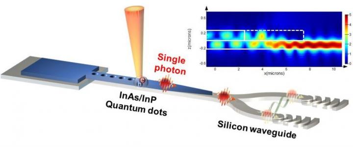
In the study, the research team demonstrated the integration of silicon photonic devices with a solid-state single photon emitter by combining silicon photonic waveguides with InAs/InP quantum dots that act as efficient sources of single photons at telecom wavelengths. Then, they removed the quantum dots via a pick-and-place procedure with a microprobe tip combined with a focused ion beam and scanning electron microscope. This technique allowed transferring of tapered InP nanobeams containing InAs quantum dots onto a silicon waveguide with nanometer-scale precision.
"This integration opens up the possibility to leverage the highly advanced photonics capabilities developed in silicon to control and route nonclassical light from on-demand single photon sources," the research team notes. "In addition, the fabricated devices operate at telecom wavelengths and can be electrically driven, which are useful for fiber-based quantum communication."
The quantum optical device, developed by the research team has successfully transferred the emission from the quantum dots along the silicon photonic circuits with high efficiency. Using this, they also successfully incorporate an on-chip silicon-photonic beamsplitter to perform a Hanbury-Brown and Twiss measurement.
"Our approach could enable integration of precharacterised III-V quantum photonic devices into large-scale photonic structures to enable complex devices composed of many emitters and photons," says Kim.


