
US team improves efficiency of nanophotonic devices
Inherent efficiency limitations of 2D hexagonal boron nitride can be overcome through careful engineering, say NRL physicists
A team of physicists, headed by the US Naval Research Laboratory (NRL), have demonstrated the means to improve the optical loss characteristics and transmission efficiency of hexagonal boron nitride (hBN) devices, enabling very small lasers and nanoscale optics.
"The applications for this research are considerably broad," said Alexander J. Giles, research physicist, NRL Electronics Science and Technology Division. "By confining light to very small dimensions, nanophotonic devices have direct applications for use in ultra-high resolution microscopes, solar energy harvesting, optical computing and targeted medical therapies."
Hexagonal BN forms an atomically thin lattice consisting of boron and nitrogen atoms. This material has recently been demonstrated as an exciting optical material for infrared nanophotonics and is considered an 'ideal substrate' for 2D materials.
While previous work demonstrated that natural hBN supports deeply sub-diffractional hyperbolic phonon polaritons desired for applications, such as, sub-diffractional optical imaging, energy conversion, chemical sensing, and quantum nanophotonics, the material has continue to show limited transmission efficiencies.
"We have demonstrated that the inherent efficiency limitations of nanophotonics can be overcome through the careful engineering of isotopes in polar semiconductors and dielectric materials," Giles said.
Naturally occurring boron is comprised of two isotopes, boron-10 and boron-11, lending a 10 percent difference in atomic masses. This difference results in substantial losses due to phonon scattering, limiting the potential applications of this material. The research team at NRL has engineered greater than 99 percent isotopically pure samples of hBN, meaning they consist almost entirely of either boron-10 or boron-11 isotopes.
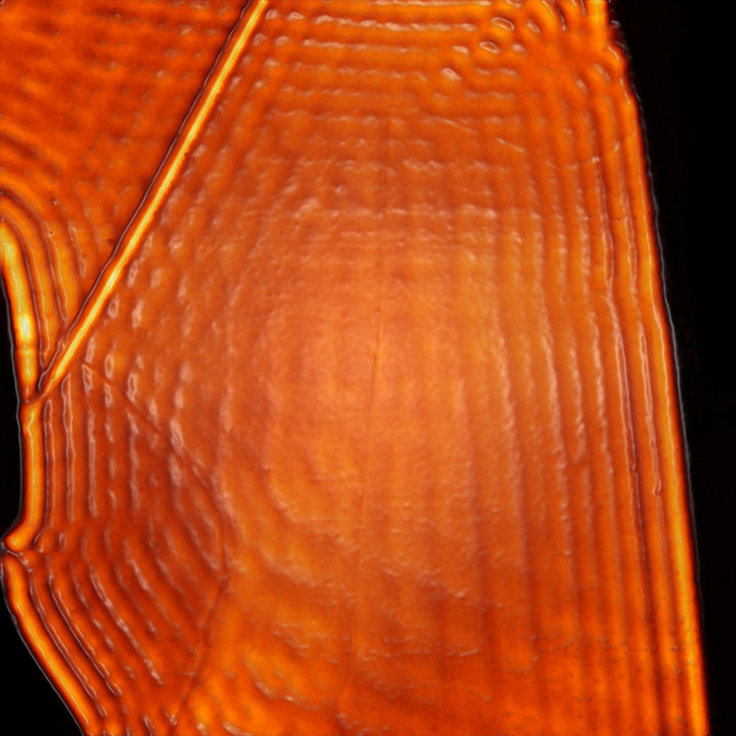
This approach results in a dramatic reduction in optical losses, resulting in optical modes that travel up to three times farther and persist for up to three times longer than natural hBN. These long-lived vibrational modes not only enable immediate advances specific to hBN - near field optics and chemical sensing - but also provide a strategic approach for other materials systems to exploit and build upon. (The image above shows directly measured polaritons propagating through a flake of hBN).
"Controlling and manipulating light at nanoscale, sub-diffractional dimensions is notoriously difficult and inefficient," said Giles. "Our work represents a new path forward for the next generation of materials and devices."


