Army scientists use InAsSb to make IR sensors

Latest research suggests a low cost solution for making night-vision systems based on III-V long wavelength IR materials
Scientists at the US Army Research Laboratory (ARL) and Stony Brook University have developed a new synthesis process for the low-cost fabrication of InAsSb for use in high sensitivity IR camera light sensors.
By using cameras that can see the faint IR light, soldiers can operate during night times. The more sensitive such a camera is, the more details that can be discerned on a battlefield at longer ranges.
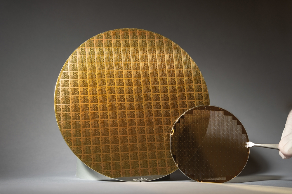
InAsSb has not been used before in cameras for the longest IR wavelengths (10 micron) but ARL's Wendy Sarney and Stefan Svensson have developed a novel approach that involves using it on GaAs as a substrate.
The best materials for IR camera light-sensors are currently based on HgCdTe, which belongs to the family of II-VI compounds."Unfortunately, they are very expensive, mostly because there are only military customers for this material," Svensson said.
Sarney and Svensson realised that InAsSb needed to be undistorted by strain in order to see at 10 microns. Also, it would need to be deposited onto a substrate with a smaller spacing between the atoms. However, this size mismatch at the atomic scale had to be managed extremely well in order for the light-sensitive material to work properly.
Over several years ARL and Stony Brook found a way to manage the atomic spacing mismatch culminating in the current work which uses GaAs as a substrate. ARL and Stony Brook combined strain-mediating techniques to effectively manage the ~10 percent atomic spacing mismatch between the InAsSb sensing material and GaAs substrate.
To do this, they deposited an intermediate layer of GaSb onto GaAs in a way that trapped most of the defects caused by the size mismatch. They then further increased the atomic spacing with a graded layer that also kept defects away from the InAsSb sensor material.
The team thinks that this is path to a practical, lower cost solution for making night-vision systems based on III-V long wavelength infrared materials.
'Bulk InAsSb with 0.1 eV bandgap on GaAs', by W. L. Sarney et al; Journal of Applied Physics 122, 025705 (2017).


