
SMI gets DOE grant for Gallium Oxide Research
Project with Carnegie Mellon researchers aims to increase the selectivity of sensors for UVA, UVB, and UVC bands
Structured Materials Industries (SMI) has received a US Department of Energy Small Business Innovation Research (SBIR) award where it will evaluate the energy bandgap tunability of Ga2O3 by alloying the material with Al2O3 and In2O3.
The ongoing effort is being conducted in collaboration with Lisa Porter and Robert Davis of Carnegie Mellon University. An assessment of the Ga2O3energy bandgap tunability is required in order to increase the selectivity of sensors for UVA, UVB, and UVC bands, which is a focus of the project. The materials are grown using MOCVD.
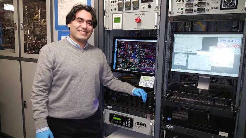
SMI research scientist and leader of Ga2O3 efforts, Serdal Okur (pictured above) commented: "Tuning the energy gap of Ga2O3 will establish an even broader range of applications for the material, such as graded heterostructures for optoelectronic devices, photo diodes(PDs) with tunable cutoff wavelengths, as well as optical filters with tunable transmission range, to name just a few.
" We believe that In2O3 and Al2O3 are good candidates to realise the bandgap engineering of Ga2O3. Additionally, we decided to use the MOCVD technique as it offers many advantages for ultimate device fabrication, including high growth rates, conformal deposition over device topography, and the capability for scale-up to high volume production."
Okur added: "In our current DOE project, SMI will demonstrate Gallium Oxide (Go), Aluminum Gallium Oxide (AlGO), and Indium Gallium Oxide (InGO) based UV sensors that cover the whole UV spectrum. In particular, these devices will be very important to detect UV photons from liquid Ar and Xe scintillators, both at 128 and 175 nm, respectively, in particle physics experiments.
"SMI will further develop the MOCVD growth parameters and hardware to extend control of energy bandgap tuning of Ga2O3 with good quality crystals. The company, in collaboration with CMU, will continue to explore the potential of large-area Ga2O3 based alloys with the intention of making the aforementioned sensors more economical and readily available than competing materials in UV sensing applications."
SMI's proprietary rotating disc oxide MOCVD reactor technology will be used in this project to demonstrate that Ga2O3 films can be deposited uniformly on large-area substrates.
SMI, with over 10 MOCVD and ALD process demonstration tools in-house, has extensive result oriented experience in providing materials, hardware, and device assistance to other businesses as well as research organisations. We are a leading provider of thin film research and development deposition systems for electronic, optical and electro-optic device fabrication.


