International team offers one-stop-shop for InP PICs

GCS, Intengent, and VLC Photonics enter into a partnership to provide one-stop fabless development services for PICs in InP
Global Communication Semiconductors (GCS), a US compound semiconductor wafer fabrication foundry; Intengent, a Canadian consultancy in the area of III-V photonics; and VLC Photonics (VLC), a photonic integrated circuit (PIC) design house based in Spain, will jointly offer fabless development into production services for customised PICs in InP (InP).
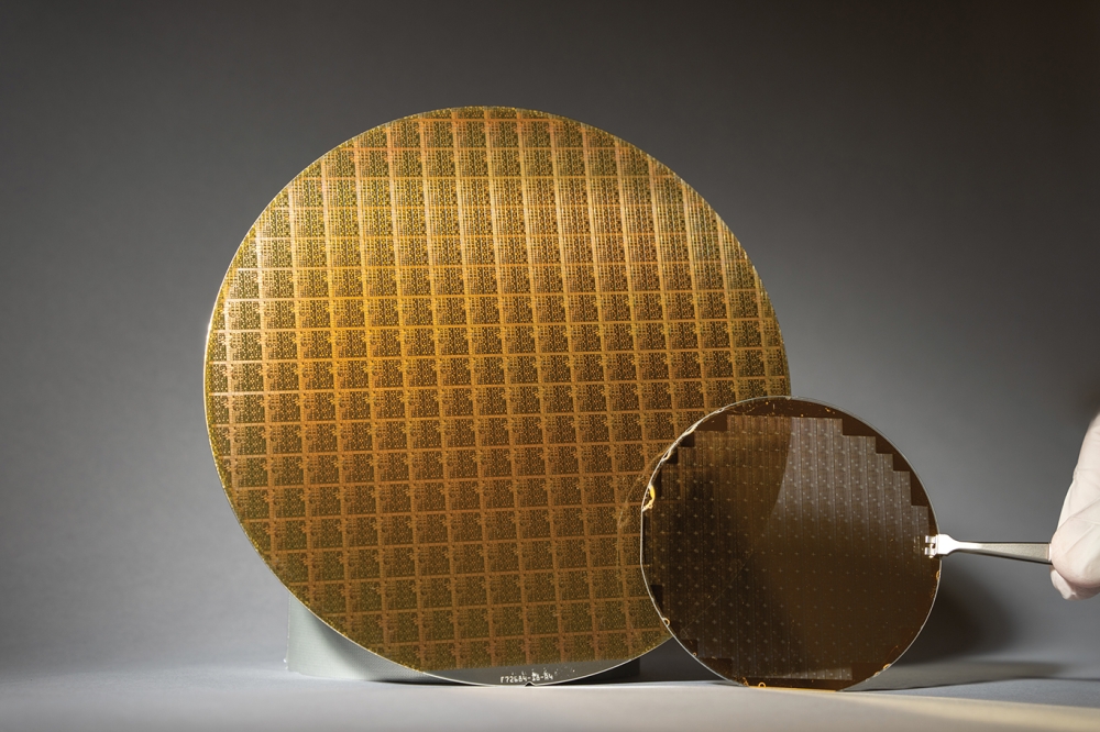
GCS provides a broad range of wafer foundry services, based on a proprietary regrowth-free process in InP. Originally developed as a state-of-the-art Opto and heterojunction bipolar transistor (HBT) processes, it also allows for prototyping and volume-scalable production of PICs. The key enabler is a photonic integration platform that is compatible with the foundry's regrowth-free process and yet suitable for a variety of applications.
Intengent has developed such a platform, termed Taper Assisted Vertical Integration (TAVI), which is regrowth-free, based on the GCS process, and enables for decoupling of epitaxial growth and wafer fabrication. TAVI covers many PIC applications, including those in growing and emerging markets, like optical interconnects and switching markets.
It also offers complimentary solutions to silicon photonics, which is considered by many the technology of choice for a high-scale integration but lacks amplifying, lasing, and other functions naturally implementable in InP. In a three-way partnership with GCS and VLC, Intengent is working towards making TAVI a generic platform while preserving its flexibility and openness to PIC customisation.
VLC Photonics is a renowned expert in generic photonic integration platforms and, as a fabless and independent design house for PICs, has been developing design libraries and process design kits (PDK) for different foundry platforms and customers. A PDK for the TAVI platform drastically reduces the PIC design effort and risk, by shifting the focus towards circuit level simulations. The evolving PDK is based on a number of verified active and passive building blocks, and is already used in commercial PIC designs carried out by the partnership.
Brian Ann, CEO of GCS, says: "Our well-established Opto and RFIC processes have great synergies with the TAVI PIC platform. Our 4", and 6" wafer capability as well, based on a commercially supplied one-step-growth epitaxy, creates a unique opportunity for PICs in InP. We truly believe that the GCS "“ Intengent "“ VLC partnership can fully utilise this opportunity and generate a significant business for PICs in various markets.
"By leveraging the infrastructure and expertise that we have gained through years of serving high-volume RF electronics and optoelectronics markets, this partnership offers time- and cost-efficient PIC development into production".
Valery Tolstikhin, CEO of Intengent, adds: "GCS is an advanced III-V foundry with a high InP wafer throughout both in RF electronics and optoelectronics markets. The TAVI platform takes advantage of GCS' process maturity and extends it to PICs in InP. To make the technology suitable for a fabless PIC development, one more thing is needed: the PDK. This is where VLC comes in, bringing a wealth of experience in PIC design and characterisation. The fabrication process, the integration platform, and the PDK, together, make a versatile generic platform for PICs in InP that allows the end users to access the commercial-grade technology under the fabless model".
"Joining with Intengent and GCS for commercialisation of the TAVI platform in a large-scale photonic foundry was a challenging but exciting experience." Iñigo Artundo, CEO of VLC, further explains. "VLC has a solid approach to working with foundries, EDA partners and customers on PDK development, based on its commercial and proprietary design tools, characterisation techniques, and in-house test and measurement capabilities. We are positive that TAVI implemented over the GCS process has a great potential as a generic platform for PICs in InP, enabling for both customisation and volume scalability in an environment of industrial-grade wafer fabrication".


