
Porous Sic: a new material for optical devices?
Viennese researchers show how 'sponge'-like semiconductors could be used to make micro-and nanomachined optical and electronic components
Researchers at TU Wien (Technical University Vienna) have succeeded in developing a method for the controlled manufacture of porous SiC. This semiconductor 'sponge' opens up new possibilities for the realisation of tiny sensors or unusual optical and electronic components.
SiC has significant advantages over silicon; it has greater chemical resistance and can therefore be used for biological applications, for example, without any additional coating required.
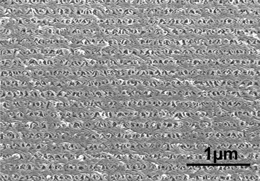
To demonstrate the potential of this new technology, a special mirror that selectively reflects different colours of light has been integrated into a SiC wafer by creating thin layers with a thickness of approximately 70 nm each and with different degrees of porosity.
Control using light refraction
"There is a whole range of exciting technical possibilities available to us when making a porous structure with countless nano holes from a solid piece of a semiconductor material," says Markus Leitgeb from the Institute of Sensor and Actuator Systems at TU Wien.
Leitgeb developed the new material processing technology as part of his dissertation with Ulrich Schmid in cooperation with CTR Carinthian Tech Research AG and sponsored by the Competence Centres for Excellent Technologies (COMET) programme.
"The porous structure influences the manner in which light waves are affected by the material. If we can control the porosity, this means we also have control over the optical refractive index of the material."
This can be very useful in sensor technology - for example, the refractive index of tiny quantities of liquid can be measured using a porous semiconductor sensor, thus allowing a reliable distinction between different liquids.
Another attractive option from a technical and application-oriented perspective is to first make certain areas of the SiC wafer porous in a highly localised manner, before depositing a new SiC layer over these porous areas, and then causing the latter to collapse in a controlled manner - this technique produces microstructures and nanostructures which can also play a key role in sensor technology.
However, in all these techniques it is crucial that the appropriate starting material is selected. "Until now, silicon has been used for this purpose, a material with which we already have a lot of experience", says Schmid.
Silicon also has significant drawbacks, however; under harsh environmental conditions, for example in extreme heat or in alkaline solutions, structures made of silicon are attacked and rapidly destroyed. Therefore, sensors made of silicon are often not suitable for biological or electrochemical applications.
For this reason, at TU Wien, attempts have been made to achieve something similar with the semiconductor SiC, which is biocompatible and considerably more robust from a chemical perspective.
Some special tricks were required, however, in order to produce porous structures from SiC.
The colour-selective mirror
First, the surface is cleaned, and then partially covered with a thin layer of platinum. The SiC is then immersed in an etching solution and exposed to UV light, in order to initiate the oxidation processes. This causes a thin porous layer - initially 1 μm thick - to form in these areas that are not coated with platinum. An electrical charge is then also applied in order to be able to precisely set the porosity and the thickness of the subsequent layers. Here, the first porous layer promotes the formation of the first pores when the electrical charge is applied.
"The porous structure spreads from the surface further and further into the interior of the material", explains Markus Leitgeb. "By adjusting the electrical charge during this process, we can control what porosity we want to have at a given depth."
In this way, it was possible to produce a complex layered structure of SiC layers with higher and lower levels of porosity, which is finally separated from the bulk material by applying a high voltage pulse. The thickness of the individual layers can be selected such that the layered structure reflects certain light wavelengths particularly well or allows certain light wavelengths to pass through, resulting in an integrated, colour-selective mirror.
"We have thus demonstrated that our new method can be used to reliably control the porosity of SiC on a microscopic scale", says Schmid.
"This technology promises many potential applications, from anti-reflective coatings, optical or electronic components and special biosensors, through to resistant supercapacitors."


