
Researchers use boron nitride to turn light upside down
Basque team has developed a technique that could be make tiny chemical sensors or manage heat in nanoscale optoelectronic devices
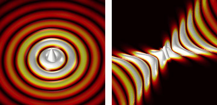
Optical waves propagating away from a point source typically exhibit circular (convex) wavefront, like the waves generated by a stone dropping in water. The reason is that the medium through which light travels is uniform in all directions.
Specifically structured surfaces can turn the wavefronts of light upside down when it propagates along them. These unusual waves are called hyperbolic surface polaritons. Because they propagate only in certain directions (with wavelengths much smaller than that of light in free space or standard waveguides) they could help to make very small optical devices for sensing and signal processing.
Researchers at nanoGUNE, a nanoscience research centre based in the Basque region of Spain, have now developed a metasurface like this for infrared light. It is based on 2D boron nitride (BN). They think it could be used to develop miniaturised chemical sensors or even used for heat management in nanoscale optoelectronic devices. The work was published this month in Science.
Hyperbolic metasurfaces are challenging to make because they need extremely precise structuring on the nanometer scale. The team mastered this challenge using electron beam lithography and etching of thin flakes of high-quality BN provided by Kansas State University.
They achieved the required precision and obtained grating structures with gap sizes as small as 25 nm. The same fabrication methods, they say, can also be applied to other materials, which could pave the way to realise artificial metasurface structures with custom-made optical properties.
(The picture above is an illustration of waves propagating away from a point-like source. Left: Regular wave propagation. Right: Wave propagation on a hyperbolic metasurface.)
To see how the waves propagate along the metasurface, the researchers used an infrared nanoimaging technique pioneered by the nanoptics group at nanoGUNE. They first placed an infrared gold nanorod onto the metasurface, which plays the role of a stone dropped into water.
The nanorod concentrates incident infrared light into a tiny spot, which launches waves that then propagate along the metasurface. With the help of a scattering-type scanning near-field microscope (s-SNOM) the researchers imaged the waves. "It was amazing to see the images. They indeed showed the concave curvature of the wavefronts that were propagating away form the gold nanorod, exactly as predicted by theory", says Rainer Hillenbrand, Ikerbasque Professor at nanoGUNE, who led the work.
The results suggest thatenanostructured 2D materials could become a novel platform for hyberbolic metasurface devices and circuits.
The research has been mainly funded by individual fellowship grants of the European Union Marie Sklodowsca-Curie Actions and the pre-doctoral research grants program of the Basque and Spanish Governments, as well as by the National Science Foundation (USA), and has been carried out in line with nanoGUNEs projects within the EU's Graphene Flagship.
'Infrared hyperbolic metasurface based on nanostructured van der Waals materials,' by Peining Li et al; Science 23 Feb 2018: Vol. 359, Issue 6378, pp. 892-896


