Loading...
News Article

Siltectra expands HQ in Dresden

News

Pilot line for laser-thinning advanced SiC, GaN, and sapphire wafers already processing customer substrates

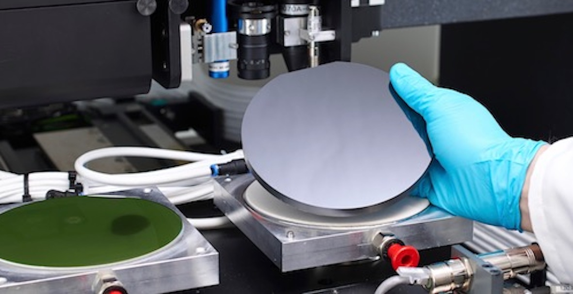
In a move that marks its shift to production, Siltectra has announced that it recently expanded its headquarters in Dresden's Technologie Park Nord and added a state-of-the-art pilot production line to the larger 900 square metre facility.

At the heart of the pilot line is the company's Cold Split laser-based wafer thinning technology, designed to cut costs for makers of devices based on advanced substrates like SiC, GaN, and sapphire, as well as silicon.

The new pilot line, which is already processing customers' substrates, is a central piece of Siltectra's growth strategy, says the company's CEO, Harald Binder.

"With the industry steadily transitioning to advanced substrates to build devices like power electronics, there is soaring interest in new technologies that can improve performance and contain costs. We're hearing daily from leading integrated device manufacturers (IDMs) who are eyeing advanced wafering technologies, in particular, to exact cost-reductions in their mass-production fabs.

This has generated high interest in our Cold Split technology. We're very pleased now to have advanced capabilities to cater to these customers."

Siltectra'S CTO, Jan Richter, added: "The pilot line gives us the critical infrastructure to accelerate our path to production and expand R&D to hit aggressive milestones on our technology roadmap. Cold Split is already out-performing traditional grinding methods by thinning wafers to 100 microns and below in minutes, with virtually no material loss.

Now, we're in final-phase testing of extended capabilities that exploit the technology's maximum potential. Results so far are very exciting. We believe that the additional innovations have the potential to deliver substantial cost savings to manufacturers of SiC-based devices."

Say hello to the heterogeneous revolution
Double heterostructure HEMTs for handsets
AlixLabs to collaborate with Linköping University
SiC MOSFETs: Understanding the benefits of plasma nitridation
Wolfspeed reports Q2 results
VueReal secures $40.5m to scale MicroSolid printing
Mitsubishi joins Horizon Europe's FLAGCHIP project
Vishay launches new high voltage SiC diodes
UK team leads diamond-FET breakthrough
GaN adoption at tipping point, says Infineon
BluGlass files tuneable GaN laser patents
QD company Quantum Science expands into new facility
Innoscience files lawsuit against Infineon
Riber revenues up 5% to €41.2m
Forvia Hella to use CoolSiC for next generation charging
Photon Design to exhibit QD simulation tool
Ortel transfers CW laser fabrication to Canada
Luminus adds red and blue multi-mode Lasers
PseudolithIC raises $6M for heterogeneous chiplet tech
Mesa sidewall design improves HV DUV LEDs
IQE revenue to exceed expectations
'Game-changing' VCSEL system targets clinical imaging
German start-up secures finance for SiC processing tech
Macom signs preliminaries for CHIPS Act funding
IQE and Quintessent partner on QD lasers for AI
EU funds perovskite tandems for fuel-free space propulsion
EU to invest €3m in GeSi quantum project
Transforming the current density of AlN Schottky barrier diodes
Turbocharging the GaN MOSFET with a HfO₂ gate
Wolfspeed launches Gen 4 SiC MOSFET technology
Report predicts high growth for UK's North East
Element Six unveils Cu-diamond composite
×
Search the news archive

To close this popup you can press escape or click the close icon.
Logo
x
Logo
×
Register - Step 1

You may choose to subscribe to the Compound Semiconductor Magazine, the Compound Semiconductor Newsletter, or both. You may also request additional information if required, before submitting your application.


Please subscribe me to:


You chose the industry type of "Other"

Please enter the industry that you work in:
 
x
Adblocker Detected
Please consider unblocking adverts on this website