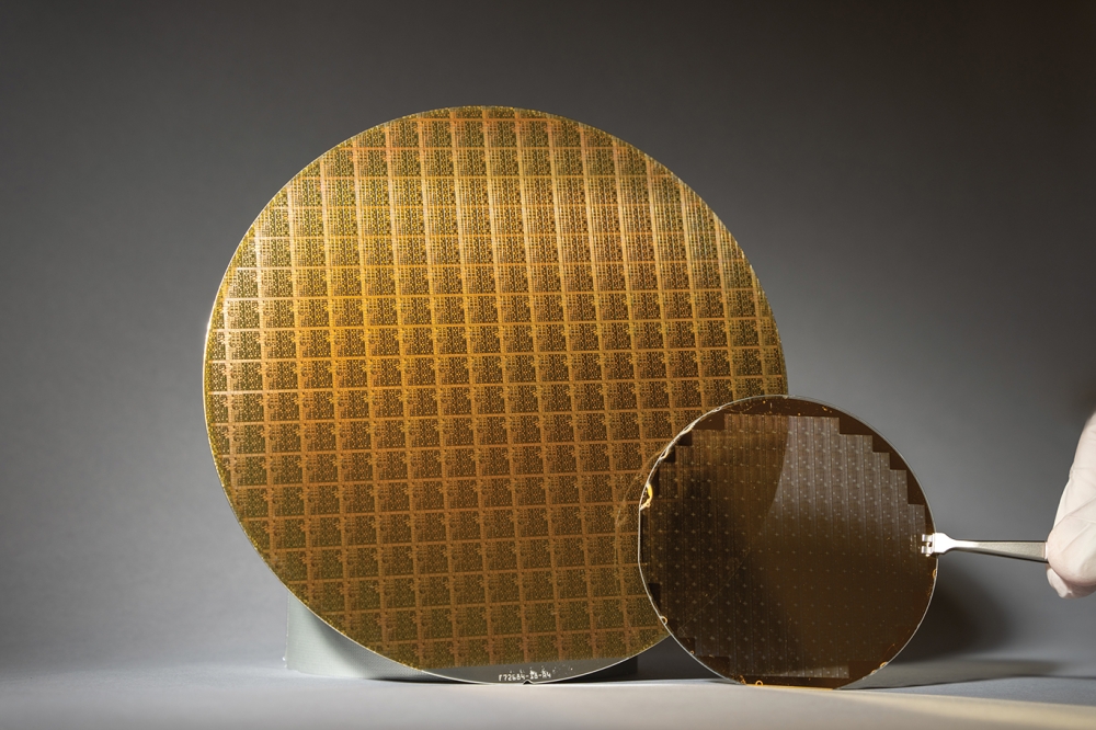
Twinning technique cuts SiC wafering costs

Siltectra validates new process by producing a GaN on SiC HEMT device on a split-off (or twinned) wafer at its new facility in Dresden
Siltectra has validated a breakthrough capability for its Cold Split, laser-based wafer-thinning technique for advanced substrates including SiC, GaN and sapphire.
Cold Split is claimed to out-performs traditional grinding methods by thinning wafers to 100 microns and below in minutes, with virtually no material loss.
Now, using an adaptation known as twinning, Siltectra has demonstrated that Cold Split can reclaim substrate material generated (and previously wasted) during backside grinding, to create a second bonus wafer in the process.
Siltectra validated the process by producing a GaN on SiC HEMT device on a split-off (or twinned) wafer at its new state-of-the-art facility in Dresden, Germany. The HEMT showed results that were superior to a non- Cold- Split-enabled HEMT when measured for CMP characterisation, as well as GaN EPI, metal layer and gate layer outcomes.
Siltectra believes that the solution's combined advantages which include fewer process steps, potentially lower equipment costs, and ultra-efficient use of substrate material, could reduce total device production costs by as much as 30 percent.
Leading integrated device manufacturers (IDMs) are now evaluating the technology.


