
Progress towards lead-free perovskite cells
Long electron-hole diffusion length in high-quality lead-free double perovskite films shows promise for solar cells
A further step has been taken along the road to manufacturing solar cells from lead-free perovskites by researchers at Linköping University (LiU), Sweden, and Nanyang Technological University in Singapore.
They have developed high quality films based on double perovskites which show promising photovoltaic properties.
Research groups around the world have recognised the potential of perovskites as one of the most promising materials for the development of cheap, environmentally friendly and efficient solar cells. In just a few years, the power conversion efficiency has increased from a few percent to over 22 percent.
The perovskites currently available for use in solar cells, however, contain lead, and Feng Gao, senior lecturer at LiU, was appointed in the autumn of 2017 as Wallenberg Academy Fellow to develop lead-free double perovskites, in which a monovalent metal and a trivalent metal replace the divalent lead.
[The general formula of perovskite is AMX3, where A is a cation, M is a divalent metal and X is a halide. Double perovskite is so named because the unit cell of is twice that of perovskite so A(n-1)M(n)X(3n+1).]
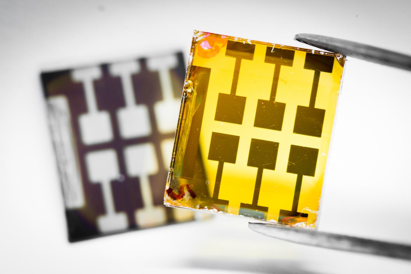
In the laboratory at the Division of Biomolecular and Organic Electronics, LiU, postdoc researchers Weihua Ning and Feng Wang have successfully manufactured single-layer thin films of densely packed crystals of double perovskites. The films are said to be of high quality and can be used as the active layer in solar cells, in which sunlight is absorbed and charge carriers created.
"Our colleagues at Nanyang Technological University in Singapore have shown that the charge carriers demonstrate long diffusion lengths in the material, which is necessary if the material is to be appropriate for application in solar cells," says Feng Gao.
The power conversion efficiency of the solar cells is still low - only around 1 percent of the energy in sunlight is converted to electricity - but neither Feng Gao or Weihua Ning are worried.
"No, we have taken the first major step and developed a method to manufacture the active layer. We have several good ideas of how to proceed to increase the efficiency in the near future," says Feng Gao.
Researchers have calculated that over 4,000 different combinations of materials can form double perovskites. They will also use theoretical calculations to identify the combinations that are most suitable for use in solar cells.
This breakthrough for research in double perovskites is also a result of the joint PhD programme in Materials- and nanoscience/technology at Linköping University and Nanyang Technological University.
"This publication is a spin-off of the discussions in relation to the joint PhD programme between NTU-LiU. Two PhD students, one on each side, have been recruited to work on this project. This is an excellent start for the program." says Tze Chien Sum from NTU.
'Long Electron"“Hole Diffusion Length in High"Quality Lead"Free Double Perovskite Films' by Weihua Ning et al; Advanced Materials 30 March 2018.


