
US scientists dig deeper into perovskite properties
Scientists led by Rice University and Los Alamos National Laboratory have discovered electronic properties in quantum-scale devices that are likely to impact the growing field of low-cost perovskite based optoelectronics.
In an open-access Nature Communications paper, researchers led by Los Alamos scientists Aditya Mohite and Jean-Christophe Blancon, both of whom will join Rice this summer, studied the behaviour of excitons trapped in quantum wells made of crystalline, halide-based perovskite compounds.
As a result, they were able to create a scale by which labs can determine the binding energy of excitons, and thus the band gap structures, in perovskite quantum wells of any thickness. This could in turn aid in the fundamental design of next-generation semiconductor materials.
Perovskite quantum well-based optoelectronic devices convert and control light at the quantum scale, reactions below 100 nanometers that follow different rules from those dictated by classical mechanics.
The excitons at the centre of their research are electrically neutral quasiparticles that only exist when electrons and electron holes bind in an insulating or semiconducting solid, like quantum wells used to trap the particles for study.
Quantum wells used in the study were synthesised by the Northwestern University lab of chemist Mercouri Kanatzidis and the Mohite Lab. They were based on perovskite compounds with a particular layered structure known as a Ruddlesden-Popper phase (RPP). This class of materials has unique electronic and magnetic properties and has found use in metal-air batteries.
"Understanding the nature of excitons and generating a general scaling law for exciton binding energy is the first fundamental step required for the design of any optoelectronic device, such as solar cells, lasers or detectors," said Mohite, who will become an associate professor of chemical and biomolecular engineering at Rice.
Previously, researchers discovered they could tune the resonance of excitons and free carriers within RPP perovskite layers by changing their atomic thickness. That appeared to change the mass of the excitons, but scientists could not measure the phenomenon until now.
"Varying the thickness of these semiconductors gave us a fundamental understanding of the quasi-dimensional, intermediate physics between monolayer 2D materials and 3D materials," said lead author Blancon, currently a research scientist at Los Alamos. "We achieved this for the first time in non-synthetic materials."
Los Alamos research scientist Andreas Stier tested the wells under a 60-tesla magnetic field to directly probe the effective mass of the excitons, a characteristic that is key for both modeling of the excitons and understanding energy transport in the 2D perovskite materials.
Bringing the samples to Rice allowed the researchers to expose them simultaneously to ultra-low temperatures, high magnetic fields and polarized light, a capability offered only by a unique spectroscope, the Rice Advanced Magnet with Broadband Optics (RAMBO), overseen by co-author and physicist Junichiro Kono.
Advanced optical spectroscopy carried out by Blancon at Los Alamos (a capability soon to be available at Rice in Mohite's lab) offered a direct probe of the optical transitions within the RPPs to derive the exciton binding energies, which is the basis of the breakthrough exciton scaling law with quantum well thickness described in the paper.
Matching their results to the computational model designed by Jacky Even, a professor of physics at INSA Rennes, France, the researchers determined that the effective mass of the excitons in perovskite quantum wells up to five layers is about two times larger than in their 3D bulk counterpart.
As they approached five layers (3.1 nanometers), Blancon said, the binding energy between electrons and holes was significantly reduced but still larger than 100 milli-electron volts, making them robust enough to exploit at room temperature. For example, he said, that would allow for the design of efficient light-emitting devices with colour tuneability.
The combined experimental and computer model data allowed them to create a scale that predicts exciton binding energy in 2D or 3D perovskites of any thickness. The researchers found that perovskite quantum wells above 20 atoms thick (about 12 nanometers) transitioned from quantum exciton to classical free-carrier rules normally seen in 3D perovskites at room temperature.
"This was a great opportunity for us to demonstrate the unique capabilities of RAMBO for use in high-impact materials research," Kono said. "With excellent optical access, this mini-coil-based pulsed magnet system allows us to perform various types of optical spectroscopy experiments in high magnetic fields up to 30 tesla."
The researchers noted that though the experiments were carried out at ultra-cold temperatures, what they observed should apply to room temperature as well.
"This work represents a fundamental and nonintuitive result where we determine a universal scaling behaviour for exciton binding energies in Ruddlesden-Popper 2D hybrid perovskites," Mohite said. "This is a fundamental measurement that has remained elusive for several decades, but its knowledge is critical before the design of any optoelectronic devices based on this class of materials and may have implication in the future for design of, for example, zero-threshold laser diodes and multifunctional hetero-material for optoelectronics."
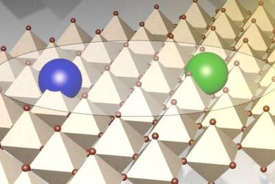
The picture above is an artist's depiction of interacting electronic charges forming a strongly bound exciton trapped in an atomic-thick layer of hybrid perovskite.


