
New Nitride holds promise for greener photovoltaics
A Tokyo Institute of Technology research team has shown copper nitride acts as an n-type semiconductor, with p-type conduction provided by fluorine doping, using a unique nitriding technique applicable for mass production and a computational search for appropriate doping elements, as well as atomically resolved microscopy and electronic structure analysis using synchrotron radiation. These n-type and p-type CuN3 semiconductors could potentially replace the conventional toxic or rare materials in photovoltaic cells.
Thin film photovoltaics have equivalent efficiency and can cut the cost of materials compared to silicon solar panels. Using the photovoltaic effect, thin layers of specific p-type and n-type materials are sandwiched together to produce electricity from sunlight. The technology promises a brighter future for solar energy, allowing low-cost and scalable manufacturing routes compared to crystalline silicon technology, even though toxic and rare materials are used in commercialised thin film solar cells.
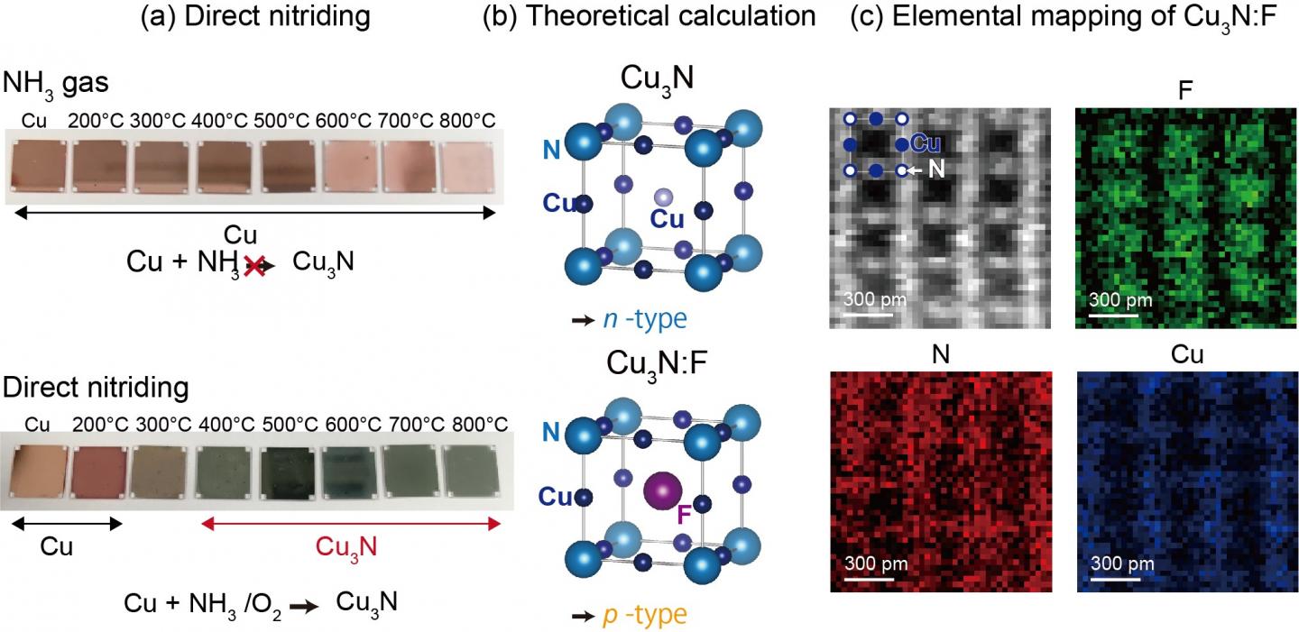
The Tokyo Institute of Technology team has challenged to find a new candidate material for producing cleaner, cheaper thin film photovoltaics. They focused on the simple binary compound, CuN3 that is composed of environmentally friendly elements. However, growing a nitride crystal in a high quality form is challenging as history tells us to develop GaN blue LEDs. Matsuzaki and his coworkers have overcome the difficulty by introducing a novel catalytic reaction route using ammonia and oxidant gas.
This compound, pictured through the photograph in figure (a), is an n-type conductor that has excess electrons. On the other hand, by inserting fluorine element in the open space of the crystal, they found this n-type compound transformed into p-type as predicted by theoretical calculations and directly proven by atomically resolved microscopy in figures (b) and (c), respectively.
All existing thin film photovoltaics require a p-type or n-type partner in their makeup of a sandwich structure, requiring huge efforts to find the best combination. P-type and n-type conduction in the same material developed by Matsuzaki and his coworkers are beneficial to design a highly efficient solar cell structure without such efforts. This material is non-toxic, abundant, and therefore potentially cheap - ideal replacements for in use CdTe and CIGS thin film solar cells.
With the development of these p-type and n-type semiconductors, in a scalable forming technique using simple safe and abundant elements, the positive qualities will further bring thin film technology into the light.


