
Highlighting Heterogenous Integration
GaN is a revolutionary material. It is behind the development of the solid-state lighting industry, it has provided the key ingredient in the Blu-ray player, and it is now starting to improve the efficiencies associated with wireless infrastructure.
In addition, there is also another legacy that GaN is leaving "“ but in this case, one that is easy to overlook. Due to the lack of affordable, widely available native substrates, GaN has shown that heterogeneous integration can yield high-quality commercial devices. Pairing GaN epilayers with either sapphire, silicon or SiC substrates has enabled the manufacture countless, reliable devices that crop up everywhere.
Where GaN has led, can GaAs and InP follow? Well, the motivation of slashing chip costs by switching to a cheaper substrate, such as silicon, still stands, but it's not so easy with those III-Vs. While GaN devices can be riddled with defects and still deliver a strong performance, that's not the case for variants based on GaAs and InP. Progress is being made, but it is lagging behind that of GaN.
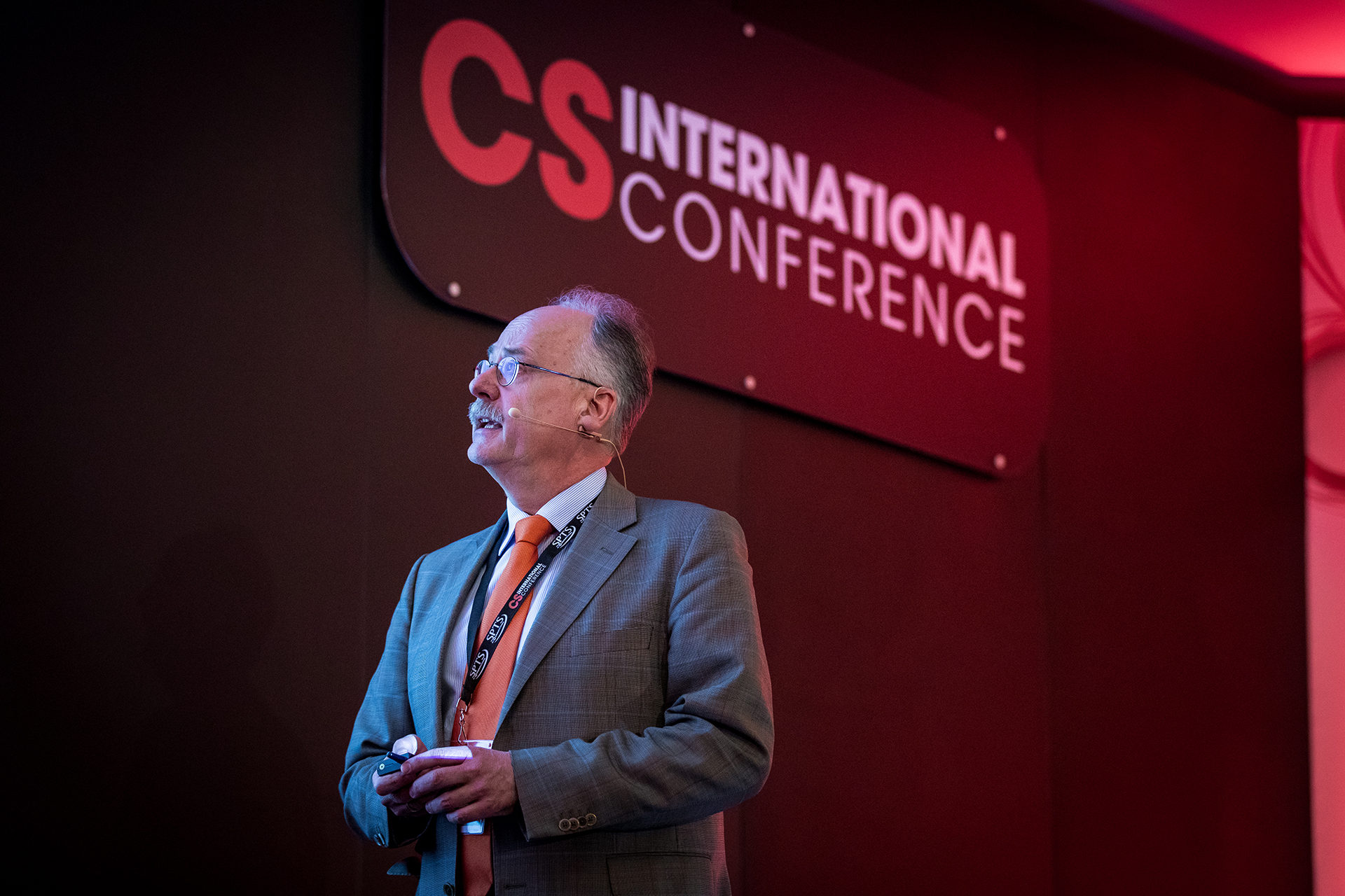
An opportunity to judge how far GaAs and InP devices are off the pace set by GaN "“ and an insight as to how far the latter has come "“ was given to delegates at this year's CS International Conference, held on 10 and 11 April at the Sheraton Airport Hotel in Brussels. At that gathering, co-located with the third Photonic Integrated Circuits International and the inaugural High End Sensors International, attendees had the chance to hear: Yole Développement's Technology and Market Analyst, Hong Lin, discuss the status and outlook of the GaN-on-silicon market; Jean-Pierre Locquet from KU Leuven detail developments in a European project aiming to deliver the dense integration of GaN power switches and CMOS drivers; Wolfgang Stolz, CTO of NAsPIII-V, outline the construction of III-V devices on CMOS-compatible silicon; and Lars-Erik Wernersson from Lund University talk about the development of III-V nanowire MOSFETs for RF and digital applications.
GaN-on-silicon success
Lin began her talk by saying that GaN, which has a 17 percent lattice mismatch with silicon and a thermal coefficient mismatch of over 50 percent, is now a mainstream technology in the power sector, a challenger in RF, and a candidate for making microLEDs.
The Yole analyst pointed out that GaN-on-silicon is no longer a new technology in the power industry. "The first devices were in 2010, by International Rectifier. Since then, other companies have come to the playground." These firms include EPC and Transphorm, which released their first GaN devices within a year or so of IR, and more recently Fujitsu, Panasonic, GaN Systems, Texas Instruments and VisIC. The majority have produced devices with blocking voltages of around 600 V, while EPC has launched a portfolio of products operating at 200 V and below.
One trend that Lin noted is a shift from discrete GaN-on-silicon power devices to power ICs. This can take the form of power devices integrated with drivers and possibly other analogue IC functions, an approach adopted by Navitas and Dialog; or a system-in-apackage, an approach taken by Texas Instruments.
Lin expects the GaN-on-silicon power market to mushroom over the next few years, with total sales climbing from $23 million in 2017 to almost $462 million in 2022. By then, sales to power supply manufacturers will be the largest sector, worth $242 million, while the electric and hybrid electric vehicle market will generate $58.9 million, and the server and data centre market $54.5 million. Despite this rapid ramp in sales, the power market for GaN-on-silicon will still be far smaller than that for GaN RF. According to Lin, global sales for GaN-onsilicon and GaN-on SiC products for RF applications will net $457 million in 2018, climbing to $1.14 billion by 2022, with revenue dominated by the military and base station markets.
Despite this rapid ramp in sales, the power market for GaN-on-silicon will still be far smaller than that for GaN RF. According to Lin, global sales for GaN-on-silicon and GaN-on SiC products for RF applications will net $457 million in 2018, climbing to $1.14 billion by 2022, with revenue dominated by the military and base station markets.
Both of these markets are performance driven, so Lin expects them to be dominated by GaN-on-SiC (see Figure 1). She argues that the best opportunities for GaN-on-silicon are in the RF energy, cable TV, and satellite markets, where this material combination can serve high-volume, cost-sensitive applications. This could help to swell sales for GaN-on-silicon RF towards $100 million by 2023.
GaN on CMOS
The keynote presentation in the heterogeneous integration session came from Jean-Pierre Locquet from the Functional Nanosystems Group at KU Leuven, who detailed the on-going GaN on CMOS project.
This four-year effort, which kicked off at the start of 2017 and is backed by €7.4 million of funding, is focused on developing novel, low-cost, reliable GaN-based processes, components, modules and integration schemes. Success on all fronts will allow the team to demonstrate the performance and economic potential of their technology at the system level, and showcase its capability to slash the energy consumed by a wide range of products, including those that require voltages of 100 V or less.
Jean-Pierre Locquet from the Functional Nanosystems Group at KU Leuven gave a keynote presentation detailing the on-going GaN-on-CMOS project.
Eleven partners are involved in the project. They are the academic institutions KU Leuven, IHP, Fraunhofer IAF, Tyndall, and several companies operating at different positions within the supply chain: EpiGaN, XFab, AT&S, NXP, Recom, PNO Innovations and IBM.
Many of the delegates may not have heard of AT&S, but it is, according to Locquet, the biggest PCB board manufacturer in Europe. Meanwhile, the most wellknown partner is the project, IBM, is hoping to benefit from its results. "They have a power issue with their servers," explained Locquet.
Figure 1. GaN-on-SiC devices operating in the RF are more plentiful, and can operate over a wider range of frequencies, compared with those based on GaN-on-silicon. Data is taken from the 2018 Yole Développement report RF GaN Market: Applications, Players, Technology and Substrates.
During the project, the team will develop ever more sophisticated techniques for unifying GaN and silicon CMOS technologies. The starting point is at the package level, with a GaN switch on top, bonded to a laminate that has inductors, capacitors and CMOS chips embedded within it. Following on from this, the team will integrate at the stack level, sandwiching the GaN switch between a laminate containing capacitors on one side, and on the other side a CMOS chip with embedded inductors. The final solution is described as a fully integrated device "“ the GaN chip is unified with the CMOS chip using a back-end-of-line process.
Locquet believes that the project will be highly innovative. Developments will include: dense integration of GaN power switches and CMOS drivers via direct wafer bonding; improvements to epiwafers, to enable a trimming of loss in switches operating below 100 V; the fabrication of normally off devices using a low temperature process; and the introduction of new soft magnetic core materials and packaging techniques that boost inductor efficiencies. In addition, Locquet provided details of how this may be accomplished, and the level of improvement wrought. He claimed that today's typical 650 V devices, which are E-mode designs that sport a cascade configuration, have figures of merit at 600 V of 5 mΩ cm2 for the product of on-resistance and current, and 0.5 nΩC for the product of on-resistance and charge. The plan is to develop 100 V devices that save energy, thanks to values of 0.1 mΩ cm2 and 0.05 nΩC.
Further gains will come from improving the process for making the GaN contact, by replacing an 800 °C step involving 30 s of annealing with one between 400 °C and 450 °C, using laser annealing. There will also be the introduction of a laminate nanocrstalline core material, rather than the standard single-plated nickel; and the replacement of a 32 nm silicon CMOS technology for making the buck convertor with a GaN-on-silicon device. These changes will enable a hike in the frequency for the voltage regulator module to more than 10 MHz, and an increase in the system power density from typically 0.09 Wmm-3 for today's GaN-based systems to more than 0.3 Wmm-3.
Locquet and co-workers are planning to produce a portfolio of demonstrators. There will be a 200 W demonstrator at the package level, a 20 W prototype at the stack level, and a 5 W device at the chip level. These devices are targeting the manufacturers of cars, airplanes, electric bikes and boats, and the builders of datacentres.
The partners are working on the development of their new technologies and processes. The project still has more than two years to run, and during that time results of working devices will start to appear.
Growing III-Vs on silicon
High-efficiency solar cells, III-V FETs, lasers and other photonic devices are all potential applications for III-Vs on silicon, according to CTO of NAsPIII-V, Wolfgang Stolz. At this year's CS International, he highlighted the capability of his company's growth technology, now pursued with an Aixtron tool that accommodates 300 mm diameter silicon wafers.
Results that showcase the company's defect-free, GaP-template technology include X-ray diffraction scans that highlight the uniformity of the material across the 300 mm-wide surface, and dark-field transmission electron microscopy images that reveal the high quality of the III-V layer. Stolz also showed atomic force microscopy scans, indicating a rootmean-square surface roughness of just 0.23 nm over a 15 μm by 15 μm area.
These defect-free, GaP-on-silicon templates have been used to produce lasers, using pseudomorphic growth. "There is no lattice mismatch, and no misfit dislocations," said Stolz, who argued that his company's technology offers the potential for producing devices with long lifetimes.
Lasers have been formed with the GaP-on-silicon templates that feature BGaAsP wafeguides and claddings, and GaNAsP quantum wells. By varying the composition and thickness of these wells, the electroluminescence peak can span the spectral domain from 850 nm to 1.2 μm.
Stolz and his co-workers have verified electrical injection with their devices, and are now working on optimising the electrical efficiency of their lasers and developing ridge waveguide structures. This could lead to the introduction of completely embedded lasers, formed by depositing the devices in recessed stripes (see Figure 2). Using this geometry could retain the planarity of the silicon wafer, and prevent cross-contamination, if silicon overgrowth and SiO2 side-wall passivation are used to hide the devices.
Nanowire MOSFETs on silicon
Within the silicon IC industry, two of the key changes since the turn of the millennium have been the introduction of new materials with a higher dielectric constant, and architectures that increase the control that the gate has over the carriers in the channel. The next step could be the use nanowires. According to Lars Wernersson from Lund University, who spoke at CS International, silicon nanowire FETs are moving towards production, while variants based on III-Vs are promising to enhance CMOS logic and RF performance.
Lars Wernersson from Lund University pointed out that new architectures and materials are needed to maintain the march of Moore's Law "“ and that III-V nanowires could have a big part of play in this evolution.
To make the case that III-Vs are no longer seen as a highly esoteric material within the silicon industry, Wernersson cited the work of TSMC, which has developed a III-V buffer on 300 mm silicon wafers and produced fin-based devices with a sub-threshold swing of around 80 mV/decade; and he recounted the efforts of a collaboration between IBM and Samsung that had produced devices with an on-current of 250 μA/μm, using a technique known as aspect ratio trapping.
Figure 2. Work at NAsPIII-V could lead to the introduction of completely embedded lasers, formed by depositing devices in recessed stripes. Merits of this approach include retaining the planarity of the silicon wafer and preventing cross-contamination.
The team from Lund has also partnered with Fraunhofer IAF. On 4-inch GaAs wafers, engineers produced 80 nm lateral MOSFETs without a spacer layer between the oxide and the channel, before using these building blocks to construct amplifiers that delivered 20 dB of gain from 75 GHz to 100 GHz.
To evaluate the capability of these devices as ICs, the researchers have teamed up with IBM and Leti. This effort has shown that III-Vs can be processed at low temperatures, using an approach the has no impact on circuits formed with a fully depleted, silicon-on-insulator technology.
Wernersson and his co-workers have also produced lateral InGaAs nanowires on InP. These devices, which are claimed to be "state of the art", sport a transconductance of 3.3 mS/μm, an on-current of 650 μA/μm at 0.5A, and a maximum oscillation frequency in excess of 400 GHz.
Back in 2017 Wernersson's team reported the results of III-V vertical MOSFETs formed with nanowires with a 28 nm diameter. These transistors, which had a 75 nm gate length, combined a transconductance of 2.4 mS/μm with an on-current of 410 μA/μm and operation at 85 mV/decade.
Vertical nanowires are used by the team from Lund, because they increase the available space for the ohmic contacts, relax the requirements for shrinking dimensions, and, according to some results, they deliver a superior performance "“ for nanowire ring oscillators, power is 35 percent higher at the 5 nm node with a vertical geometry.
Continuing in this vein, Wernersson and his coworkers are developing III-V FETs that feature a nanowire. Merits of this one-dimensional structure include advantageous transport and a wrap gate geometry "“ enabling a high transconsductance, high drive current, and a low output conductance. What's more, nanowires have a small footprint. "This avoids defect propagation from the surface," argued Wernersson.
Yole Développement's Technology and Market Analyst, Hong Lin, told delegates at CS International that she expects the GaN-on-silicon power market to grow very fast over the next few years, with total sales climbing from $23 million in 2017 to almost $462 million in 2022.
Wernersson and co-workers have also explored tunnel FETs. Vertical InAs-based devices with nanowire widths of 88 nm and 63 nm have produced sub 60 mV/decade operation at drive currents ranging from 1 nA/μm to 300 nA/μm, along with good electrostatic control.
The efforts of the team from Lund, and other developers of compound semiconductor devices on silicon, show that the benefits of this form of heterogeneous integration can be exploited. Sales of these devices are sure to rise over the coming years.


