
Nano-imaging of intersubband transitions in 2D materials
Semiconducting heterostructures have been key to the development of electronics and opto-electronics. Many applications in the infrared and terahertz frequency range exploit transitions, called intersubband transitions, between quantised states in semiconductor quantum wells. These intraband transitions exhibit very large oscillator strengths, close to unity. Their discovery in III-V semiconductor heterostructures depicted a huge impact within the condensed matter physics community and triggered the development of quantum well infrared photodetectors as well as quantum cascade lasers.
Quantum wells of the highest quality are typically fabricated by molecular beam epitaxy (sequential growth of crystalline layers), which is a well-established technique. However, it poses two major limitations: Lattice-matching is required, restricting the freedom in materials to choose from, and the thermal growth causes atomic diffusion and increases interface roughness.
2D materials can overcome these limitations since they naturally form a quantum well with atomically sharp interfaces. They provide defect free and atomically sharp interfaces, enabling the formation of ideal QWs, free of diffusive inhomogeneities. They do not require epitaxial growth on a matching substrate and can therefore be easily isolated and coupled to other electronic systems such as silicon CMOS or optical systems such as cavities and waveguides.
Surprisingly enough, intersubband transitions in few-layer 2D materials had never been studied before, neither experimentally nor theoretically. Thus, in a recent study published in Nature Nanotechnology, ICFO researchers Peter Schmidt, Fabien Vialla, Mathieu Massicotte, Klaas-Jan Tielrooij, Gabriele Navickaite, led by ICREA Prof at ICFO Frank Koppens, in collaboration with the Institut Lumière Matière - CNRS, Technical University of Denmark, Max Planck Institute for the Structure and Dynamics of Matter, CIC nanoGUNE, and the National Graphene Institute, report on the first theoretical calculations and first experimental observation of inter-sub-band transitions in quantum wells of few-layer semiconducting 2D materials (TMDs).
In their experiment, the team of researchers applied scattering scanning near-field optical microscopy (s-SNOM) as an innovative approach for spectral absorption measurements with a spatial resolution below 20 nm. They exfoliated TMDs, which comprised terraces of different layer thicknesses over lateral sizes of about a few micrometers. They directly observed the intersubband resonances for these different quantum well thicknesses within a single device. They also electrostatically tuned the charge carrier density and demonstrated intersubband absorption in both the valence and conduction band. These observations were complemented and supported with detailed theoretical calculations revealing many-body and non-local effects.
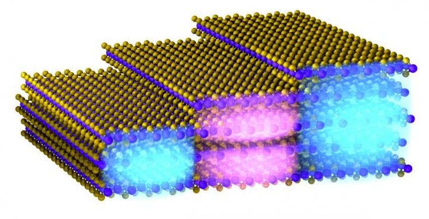
The schematic illustration above shows charge carriers confined within a TMD flake comprising different thicknesses. Charge carriers in the ground state (blue) can be excited upon resonant light excitation to a higher state (pink).
The results of this study pave the way towards an unexplored field in this new class of materials and offer a first glimpse of the physics and technology enabled by intersubband transitions in 2D materials, such as infrared detectors, sources, and lasers with the potential for compact integration with silicon CMOS.


