Supercomputer predicts perovskite hybrid optical properties

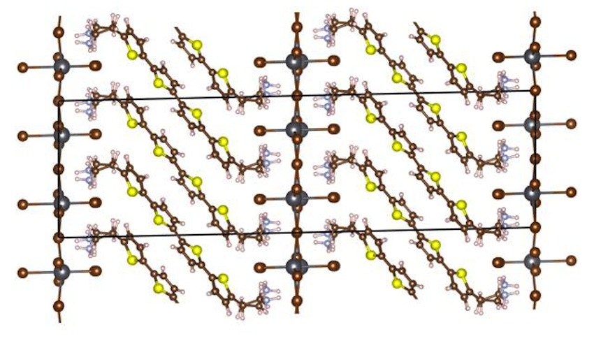
Materials scientists at Duke University in the US have computationally predicted the electrical and optical properties of semiconductors made from layered hybrid organic-inorganic perovskites - or HOIPs (pictured above).
HOIPs are popular targets for light-based devices such as solar cells and LEDs. The ability to build accurate models of these materials atom-by-atom will allow researchers to explore new material designs for next-generation devices. The results appeared online on October 4 in Physical Review Letters.
"Ideally we would like to be able to manipulate the organic and inorganic components of these types of materials independently and create semiconductors with new, predictable properties," said David Mitzi, the Simon Family Professor of Mechanical Engineering and Materials Science at Duke. "This study shows that we are able to match and explain the experimental properties of these materials through complex supercomputer simulations, which is quite exciting."
HOIPs are a promising class of materials because of the combined strengths of their constituent organic and inorganic pieces. Organic materials have more desirable optical properties and may be bendable, but can be ineffective at transporting electrical charge. Inorganic structures, on the other hand, are typically good at conducting electricity and offer more robust mechanical strength.
Combining the two can affect their individual properties while creating hybrid materials with the best of both worlds. Understanding the electronic and atomic-scale consequences of their interaction, however, is challenging at best, since the resulting crystals or films can be structurally complex. But because these particular HOIPs have their organic and inorganic components in well-ordered layers, their structures are somewhat easier to model, and researchers are now beginning to have success at computationally predicting their behaviors on an atomic level.
"The computational approach we used has rarely been applied to structures of this size," said Volker Blum, associate professor of mechanical engineering and materials science and of chemistry at Duke. "We couldn't have done it even just ten years ago. Even today, this work would not have been possible without access to one of the fastest supercomputers in the world."
That supercomputer - dubbed Theta - is currently the 21st fastest in the world and resides at Argonne National Laboratory. The group was able to gain time on the behemoth through Blum securing one of only a dozen Theta Early Science Projects, aimed at paving the way for other applications to run on the system first launched in late 2017. They are now co-investigators on one of Department of Energy's "˜Innovative and Novel Computational Impact on Theory and Experiment' (INCITE) awards, enabling them to continue their work.
In the new study, Chi Liu, a graduate student in Blum's laboratory; Yosuke Kanai, a fellow theorist at the University of North Carolina - Chapel Hill; and Alvaro Vazquez-Mayagoitia, a scientist at Argonne National Laboratory, used Theta's computational power to model the electronic states within a layered HOIP first synthesized by Mitzi more than a decade ago. While the electrical and optical properties of the material are well-known, the physics behind how they emerge have been much debated.
The team has now settled the debate.
In a series of computational models, the team calculates the electronic states and localises the valence band and conduction band of the HOIP's constituent materials, the organic bis(aminoethyl)-quaterthiophene (AE4T) and PbBr4. These properties dictate how electrons travel through and between the two materials, which determines the wavelengths and energies of light it absorbs and emits, among other important properties such as electrical conduction.
The results showed that the team's computations and experimental observations match, proving that the computations can accurately model the behaviours of the material.
Liu then went further by tweaking the materials - varying the length of the organic molecular chain and substituting chlorine or iodine for the bromine in the inorganic structure - and running additional computations. On the experimental side, Mitzi and collaborator Wei You, professor of chemistry and applied physical sciences at the University of North Carolina - Chapel Hill, are working on the difficult task of synthesising these variations to further verify their colleagues' theoretical models.
The work is part of a larger initiative called the HybriD3 project aimed at discovering and fine-tuning new functional semiconductor materials. The collaborative effort features a total of six teams of researchers. Joining those researchers located at Duke University and the University of North Carolina at Chapel Hill, professors Kenan Gundogdu and Franky So at North Carolina State University are working to further characterise the materials made in the project, as well as exploring prototype light-emitting devices.
"By using the same type of computation, we can now try to predict the properties of similar materials that do not yet exist," said Mitzi. "We can fill in the components and, assuming that the structure doesn't change radically, provide promising targets for materials scientists to pursue."
This ability will allow scientists to more easily search for better materials for a wide range of applications. For this particular class of materials, that includes lighting and water purification.
Inorganic light sources are typically surrounded by diffusers to scatter and soften their intense, concentrated light, which leads to inefficiencies. This class of layered HOIPs could make films that achieve this more naturally while wasting less of the light. For water purification, the material could be tailored for efficient high-energy emissions in the ultraviolet range, which can be used to kill bacteria.
"The broader aim of the project is to figure out the material space in this class of materials in general, well beyond the organic thiophene seen in this study," said Blum. "The key point is that we've demonstrated we can do these calculations through this proof of concept. Now we have to work on expanding it."
"˜Tunable Semiconductors: Control Over Carrier States and Excitations in Layered Hybrid Organic-Inorganic Perovskites' by Chi Liu et al; Phys. Rev. Lett., 121, 146401, 2018


