Loading...
News Article

InnoScience powers GaN development with Aixtron

News
AIX G5+ C high-volume manufacturing platform paves way to high-performing 650V GaN-on-Si devices

Aixtron SE will deliver multiple AIX G5+ C MOCVD systems to InnoScience Technology (China) for the development of GaN power devices. All Aixtron cluster tools will feature a 5x200 mm configuration and will be shipped until Q2/2019.

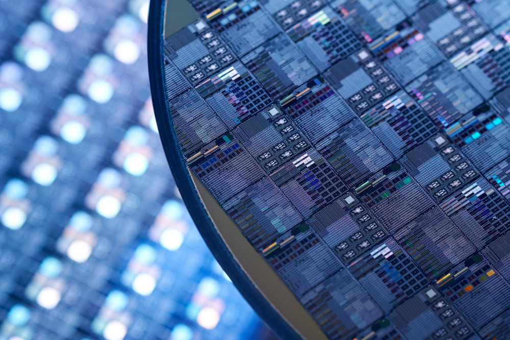
Innoscience Technology was co-founded in December 2015 by scientists and experts from the US, Korea, Taiwan, and China. It is devoted to the R&D and manufacture of wide-bandgap semiconductors. The first fab is located in Zhuhai National Hi-Tech District (China). Innoscience has established China’s first mass production line of 8-inch E-mode GaN-on-Si power devices.

Jay Son, CEO of InnoScience Technology, says: "We have chosen the AIX G5+ C as it has proven to provide excellent thickness and wafer uniformity due to the superior capabilities of the Planetary® batch reactor concept. The newly acquired systems will enable us to ramp up manufacturing of our high-end products such as 650V GaN-on-Si devices with the best cost per wafer in the market."

"Market demand for power electronics, especially for GaN-based devices is picking up speed with Aixtron having the most capable system available in the market. We are pleased that InnoScience leads the way in China and has decided to select this system which convinces not only by performance but also by making the production of GaN power devices commercially viable," comments Felix Grawert, president of Aixtron SE.

Double heterostructure HEMTs for handsets
AlixLabs to collaborate with Linköping University
SiC MOSFETs: Understanding the benefits of plasma nitridation
Wolfspeed reports Q2 results
VueReal secures $40.5m to scale MicroSolid printing
Mitsubishi joins Horizon Europe's FLAGCHIP project
Vishay launches new high voltage SiC diodes
UK team leads diamond-FET breakthrough
GaN adoption at tipping point, says Infineon
BluGlass files tuneable GaN laser patents
QD company Quantum Science expands into new facility
Innoscience files lawsuit against Infineon
Riber revenues up 5% to €41.2m
Forvia Hella to use CoolSiC for next generation charging
Photon Design to exhibit QD simulation tool
Ortel transfers CW laser fabrication to Canada
Luminus adds red and blue multi-mode Lasers
PseudolithIC raises $6M for heterogeneous chiplet tech
Mesa sidewall design improves HV DUV LEDs
IQE revenue to exceed expectations
'Game-changing' VCSEL system targets clinical imaging
German start-up secures finance for SiC processing tech
Macom signs preliminaries for CHIPS Act funding
IQE and Quintessent partner on QD lasers for AI
EU funds perovskite tandems for fuel-free space propulsion
EU to invest €3m in GeSi quantum project
Transforming the current density of AlN Schottky barrier diodes
Turbocharging the GaN MOSFET with a HfO₂ gate
Wolfspeed launches Gen 4 SiC MOSFET technology
Report predicts high growth for UK's North East
Element Six unveils Cu-diamond composite
SemiQ launches hi-rel 1700V SiC MOSFETs
×
Search the news archive

To close this popup you can press escape or click the close icon.
Logo
x
Logo
×
Register - Step 1

You may choose to subscribe to the Compound Semiconductor Magazine, the Compound Semiconductor Newsletter, or both. You may also request additional information if required, before submitting your application.


Please subscribe me to:


You chose the industry type of "Other"

Please enter the industry that you work in: