
European InP PIC pilot project takes off
Twelve partners from northwestern Europe are creating an open access PIC (photonic integrated circuit) pilot line that it is claimed will drastically reduce costs and time for the pilot production of new products. This new facility is projected to be the incubator of a thousand new companies and thousands of jobs. The €14 million project (OIP4NWE) is supported by the European Regional Development Fund.
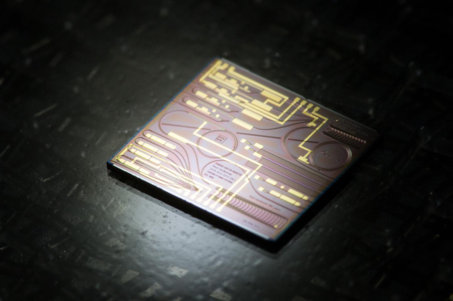
One of the main hurdles for PIC production is the high cost involved in R&D. Not only does it require expensive high-tech equipment installed in cleanrooms, but currently the production processes still have a high defect rate and are too slow. This was workable for basic research but not for commercial R&D.
The new project, led by photonics stronghold Eindhoven University of Technology (in collaboration with its Photonic Integration Technology Centre), consists of the realisation of an efficient pilot production line for shared use by European SMEs. It should take the defect rate in pilot production down and the throughput time will be shorter. All in all, this should lead to a cost reduction which significantly lowers the threshold for developing new photonic products. This should help establish a thousand integrated photonics firms within ten years after the project.
The front-end process (production of PICs on InP wafers) will be realised in the existing NanoLab at Eindhoven University. The PICs of different companies will be combined on one wafer to keep costs low. The back-end process is done at the Vrije Universiteit Brussel (Optics for beam shaping and light coupling) and at the Irish Tyndall National Institute (Assembly of fibre-optic connections and electronics in the package). All steps require nanoscale precision to avoid product defects.
The first stage of the project is equipment installation. The second stage focusses on automation of the equipment while a third stage will involve intensive industrial research together with equipment manufacturers to optimise and develop new processes. The line should be fully in operation in 2022. To incentivise the initial uptake by SMEs, a voucher scheme for external SMEs will be set up.
The other parties involved are the companies Aixtron SE (Germany), SMART Photonics, VTEC Lasers & Sensors, Technobis Fibre Technologies (all Netherlands), mBryonics Limited (Ireland) and Oxford Instruments nanotechnology Tools (United Kingdom) along with research centres Photonics Bretagne (France), Cluster NanoMikroWerkstoffePhotonik.NRW (Germany) and Photon Delta Cooperatie (Netherlands).
The project has a total budget of €13.9 million. Of this, the EU is funding €8.3 million, with the remainder coming from the participating parties.


