
Allos customers confirm benefits of GaN-on-Si process
Absence of C-doping reduces switching losses at high frequencies by reducing electron-trapping effects
Dresden-based GaN-on-Si technology licensing firm Allos Semiconductor has announced customer feedback on the outstanding wafer-level data, excellent dynamic Ron and high temperature performance of its GaN-on-Si technology.
It confirms the benefits of avoiding carbon-doping according to Allos’ co-founder and CTO Atsushi Nishikawa who showed the data and the underlining analysis at an invited talk at the E-MRS scientific conference in Warsaw.
Being able to make this proof is important for the high power electronics industry because it confirms the widespread believe that the absence of C-doping can help reduce switching losses at high frequencies (dynamic Ron) by reducing electron-trapping effects. Nevertheless, C-doping is usually unavoidable to achieve the required breakdown voltage but it causes lower crystal quality and with that more trapping and reliability issues.
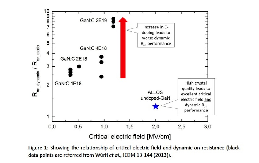
Allos has therefore overcome this challenge of delivering other crucial performance parameters at the same time by showing - on the same epiwafer not only good dynamic Ron - but also the renowned good crystal quality and extremely low leakage of Allos.
Nishikawa explains: “In epitaxy you often need to work with trade-offs between different criteria and thus it is really a big success to achieve all required specification parameters at the same time”.
Figure 1 shows the relationship of critical electric field and dynamic on-resistance (black data points are referred from Würfl et al., IEDM 13-144 (2013)).
“It is Allos’ value proposition to deliver a technology platform addressing all required spec parameters at the same time to enable our customers to make such epiwafers themselves after a technology transfer from us in only 12 weeks” is added by Alexander Loesing, cofounder and CMO of Allos.
In addition to excellent dynamic Ron and leakage performance, the 150 and 200 mm epiwafers have controlled and flat bow - and through the availability in SEMI-standard thicknesses, the epiwafers are suitable for processing in high volume CMOS lines.
Based on its business model, Allos continues making its epiwafer technology available to high power electronic companies who would like to enter the GaN-on-Si business and avoid the cost, risk and uncertainty of starting their own epi development from scratch.
“At the same time also customers who already have an ongoing GaN-on-Si activity can benefit. In some cases they are not yet completely happy with their performance or want to increase the voltage range of their products to 1200 V”, adds Loesing and he further cites that in particular wafer breakage is a key problem still faced by many. Focusing on the low risk which Allos offers its customers by guaranteeing the performance delivered in a technology transfer, he adds: “And of course customers can test the technology easily by buying epiwafer samples from us.”


