
SUSS opens Excellence Centre in Switzerland
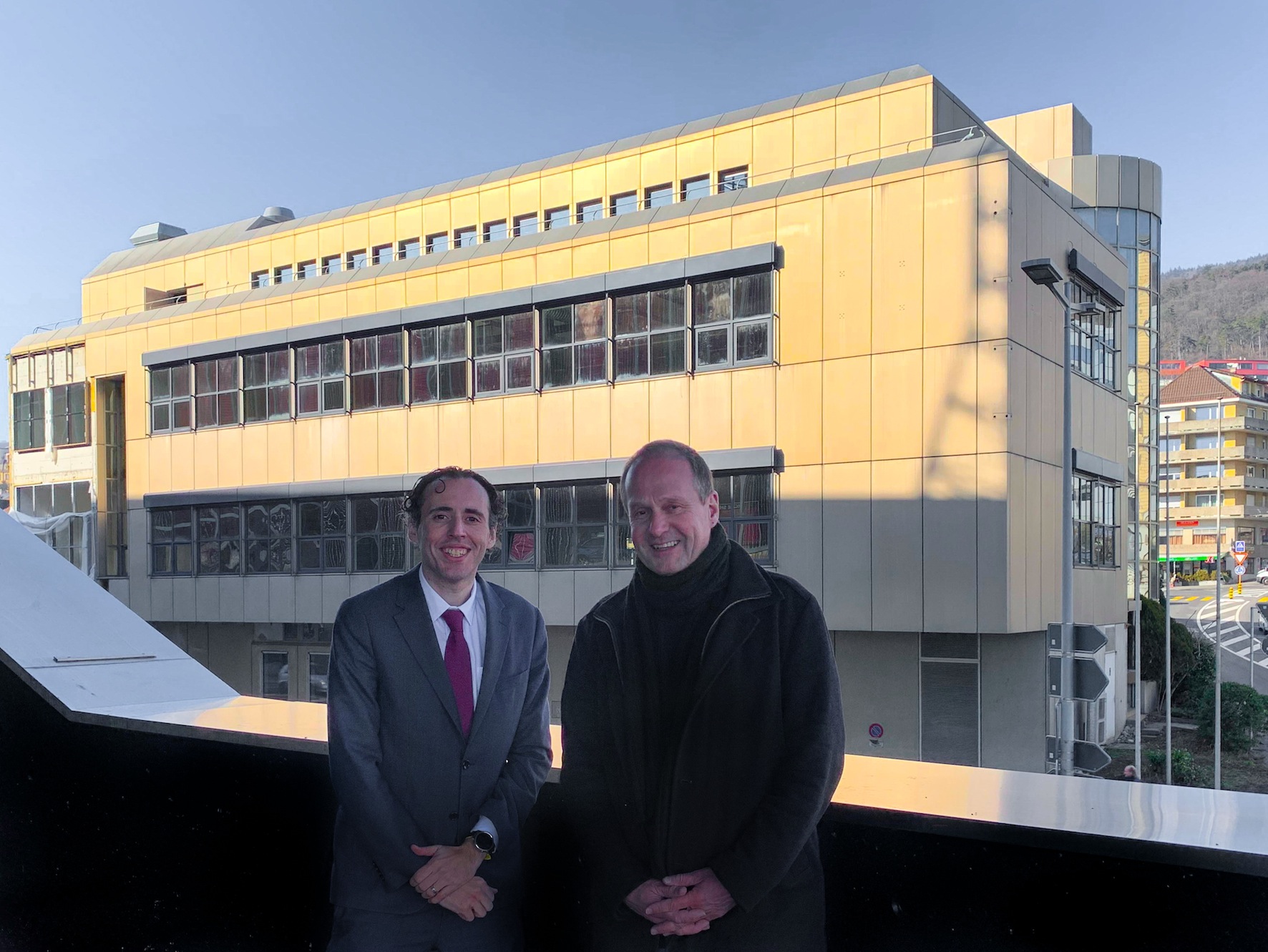
Reinhard Völkel (CEO at SUSS MicroOptics) and Jose Pozo (CTO at EPIC-European Photonics Industry Consortium)
SUSS MicroOptics is setting up an excellence centre in Neuchâtel Switzerland for manufacturing wafer-level optics (WLO) in order to meet the increase in demand for precision optics applications.
Among the various structures that can be manufactured at wafer-level, freeform micro-optic arrays are one of the most challenging, as they have no rotational symmetry. Thanks to this property, they can generate new light distribution patterns, correct for aberrations, as well as improve miniaturisation of the optical systems. This will be key for driving the volume production of new optics for volume markets such as automotive, transportation, lighting, augmented reality, medical, datacom, consumer electronics etc. The excellence centre will be part of 800m2 of new cleanroom space currently built in Neuchâtel and certified for the main markets targeted by SUSS MicroOptics.
The European photonic industry Consortium (EPIC) has consistently shown strong support for European funded Photonics Pilot Lines manufacturing photonic devices. EPIC is already the dissemination partner of the MIRPHAB pilot lines (manufacturing of MID-IR photonics sensors), PIXAPP (manufacturing of packaged integrated photonic devices) and InPULSE (manufacturing of photonic integrated circuits based InP).
Jose Pozo, EPIC's CTO, claims "these European pilot lines, whether funded or not by the EU, are essential for the exploitation of the great innovations in photonics in Europe. Photonics21 and the Photonics public private partnership, are playing the necessary role for manufacturing of Photonics, as a key enabling technology, in Europe. We strongly believe that such pilot lines are the best way of enabling the manufacturing of photonics in Europe to customers worldwide and of valorising and monetising the photonics innovations which have positioned Europe in the lead of photonics R&D."
The expertise of SUSS MicroOptics, based on imprint technologies, enables the production of the last mile in optics: the so-called freeform micro-optics, mainly optical diffractive, refractive or reflective components with no rotational symmetry. Until now most freeform optics applications have been in niche markets, such as space and others. Recently however, high volume applications in consumer markets especially in automotive, mobile phones, lighting and high-end cameras have emerged.
According to SUSS MicroOptics, the goal is to enable volume manufacturing from pilot production all the way to high-volume production in Europe and in particular in Neuchâtel. Neuchâtel was chosen as the location because of the city's long-standing connection with the high-end watch industry and its role in transforming expensive, low-volume technologies to higher volumes, keeping high quality standards while reducing costs.
CSEM, a Research Technology Organisation (RTO), has traditionally been the link between R&D lines and user applications. Rolando Ferrini, Section Head MicroNano Optics & Photonics at CSEM has been appointed in charge of linking wafer -level R&D lines to volume manufacturing. As he says: "finding synergies between the huge technological developments in wafer-level micro-optics, which have happened in Europe in the last decade, mostly funded by European H2020 grants and regional funds, positions today Europe as a leader in bringing freeform micro-optics to higher volumes: it is now or never to create volume manufacturing capabilities in Europe in this strategic field, which is foreseen to have strong impact in several application domains."
The SUSS Excellence Centre will use SUSS MicroTec's manufacturing equipment to provide manufacturing services which can be scaled up to contract manufacturing. SUSS MicroOptics CEO, Reinhard Völkel says: "the best way of bringing high-quality freeform micro-optics in applications such as microlens arrays for cameras, is to prove the pilot production of such micro-optics in Neuchâtel and other locations in Europe. The goal must be to convince high-volume companies that they can start pilot production with us and scale to volume production either by licensing or by replicating SUSS's production process in their own facilities by using European equipment. This is key for European innovation and most importantly for the smart use of R&D innovation funds"


