

Refining SiC epi-growth for high-volume production
Screening the substrate, optimising a fast growth process and going slow in the cool-down step are three ingredients to high-yield, high-volume production of SiC epiwafers
BY NICOLÒ PILUSO FROM STMICROELECTRONICS
SiC has many great attributes, making it a very promising material for numerous applications. Its low intrinsic carrier concentration and high thermal conductivity make it a strong candidate in the automotive sector; its combination of a low thermal expansion coefficient, high hardness and tremendous linearity in harsh environments give it great potential in uses related to astronomy; and its high band gap, high drift velocity and high breakdown voltage are enabling it to succeed in the power electronics market.
To ensure that SiC can excel in all these sectors, there is a need for high-yield manufacturing of devices with a high crystal quality. That means that the SiC epilayers that are grown on the substrate, usually 4H-SiC, must combine a high degree of uniformity across the wafer with a low defect density, as well as thicknesses and doping concentrations that hit their target values.
Our team at the STMicroelectronics R&D Group and Production Group in Catania, Italy, can excel on all these fronts, due to our expertise in developing SiC growth processes for high-volume, high-yield production of high-performance power devices.
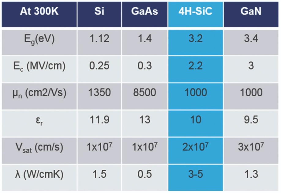
Table 1. SiC has a great set of attributes.
We have built on the successes of the pioneers of epitaxy, and in particular on those that have broken new ground with SiC epitaxy. Their milestones include: the first crystal growth method made by Jan Czochralski in 1916 and used by Siemens in 1951 and by Texas Instruments 1952 to produce the first high-purity silicon wafers; the first transistor, made in germanium in 1947 by John Bardeen and William Brattain at Bell Labs; the first silicon MOSFET, made by Martin “John” Atalla and Dawon Kahng at Bell Labs in 1959; the first stable growth method for a SiC ingot made by Yuri Tairov and Valeri Tsvetkov in 1978 at the Institute of Electrical Engineering of Leningrad; and the first excellent results, reported in 1987, of CVD reactor growth for 6H and 4H-SiC, made by Hiroyuki Matsunam’s group at Kyoto University. Our contributions are our insights into realising excellent material quality through optimised etching of substrate, the growth of drift layers with an ultra-low defect density, and a slow cool-down process for the chamber.Heating the wall
The most common reactor for the growth of 4H-SiC homoepitaxial layers is the Hot Wall CVD (HWCVD) reactor. Its primary advantages over cold wall designs are its low thermal gradient, the long lifetime of the susceptor and the low back-deposition. For high-volume manufacture, horizontal reactors with a rotating holder are preferred, because they drive down production costs.
SiC epilayers are formed by introducing silicon and carbon precursors into a chamber containing substrates heated to around 1600 °C. The precursors are decomposed and atoms of silicon and carbon impinge on the substrates, migrate and bind together to form SiC epilayers (see Figure 1, which highlights the main chemical reactions occur during the epitaxial growth, as well as the design of the HWCVD tool).
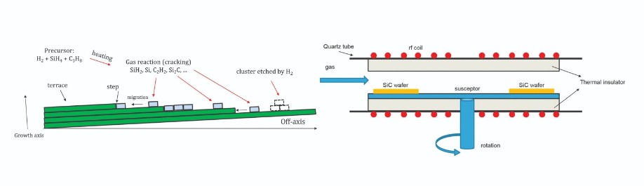
Figure 1. (left) Decomposition of precursors on the substrate surface, followed by migration of atoms, leads to 4H-SiC homoepitaxy growth. (right) Growth of SiC epiwafers is most commonly undertaken in a horizontal hot-wall CVD reactor.
High-quality epilayers result from stabilizing and optimising the temperature and pressure within the reactor. The fine-tuning of these levers leads to ideal conditions for the migration of the species, and the growth of the crystal. To realise a high throughput, up to eight wafers are loaded on a susceptor. Rotation ensures uniformity, in terms of thickness and doping. A greater challenge is the realisation of a low defect density in the epilayers.Eradicating defects
Many different classes of defect can plague SiC epilayers (see Figure 2 for an overview). These imperfections arise from either a local instability in temperature or pressure, a non-optimal balance of silicon and carbon precursors, or a slow growth rate. To ensure good material quality, it is also imperative to grow the epilayers on a high-quality substrate.
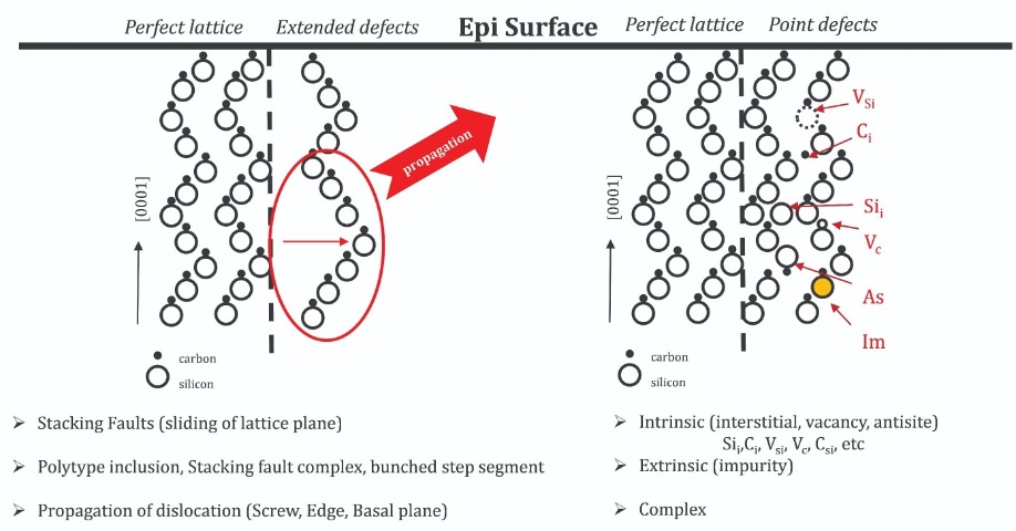
Figure 2. The defects that occur during 4H-SiC homoepitaxy can be sub-divided into extended and point defects.
One of the most well-known extended defects in SiC is the stacking fault. It is generated by the sliding of a basal plane. This creates a crystal superlattice with local parameters that deviate from those of 4H-SiC and compromise device performance.Other forms of extended defect include polytype inclusions, and dislocations that propagate. The inclusion of 3C and 6H polytypes, which can occur during the epi-growth, may change local, fundamental parameters of the host semiconductor, such as the band edge, thermal conductivity and carrier lifetime. This leads to drastically degraded electrical characteristics. Dislocations can also be disastrous, shortening the local carrier lifetime – and in cases where pits propagate, accelerating deterioration of the oxide. One imperfection of this form is the carrot defect, which is predominantly generated by a threading screw dislocation propagating in the substrate. There are also triangles, an extended defect that originates from the presence of particles or carbon inclusions on the surface during growth.
As well as all these forms of extended defect, there are point defects. They act as trap centres, and when they are found in MOSFETs, they impair channel mobility, decrease carrier lifetime and cause a hike in the reverse-bias current.
There is no quick fix to addressing all these imperfections. What’s needed is a comprehensive, careful study of what the potential pitfalls are at every step of the epitaxial process, and how they can be avoided. Such a study must consider the impact of time, precursor ratios, temperature, pressure, and gas carriers, not only on the growth steps, but also on the loading and unloading of the wafers (as illustrated in Figure 3).
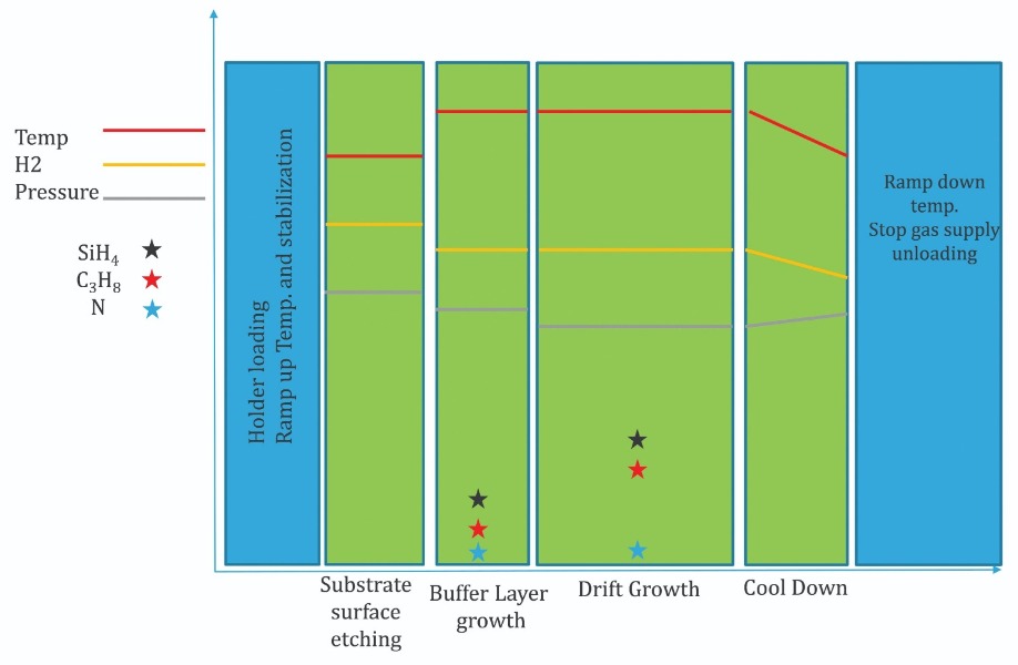
Figure 3. The growth of SiC devices by CVD involves surface etching, the growth of buffer and drift layers, and a cool down step.
Before growth commences, the surface of the substrates is cleaned by hydrogen etching. Optimising the time for this process holds the key to reducing defects. That’s not easy: longer times improve thickness uniformity, but at the expense of higher defect densities and degradation in doping uniformity (see Figure 4).We have devoted much effort to trimming the etching time below 10 minutes, in order to cut the defect density and increase doping uniformity. The decline in thickness uniformity can be kept in check by raising the temperature, because this bolsters the effectiveness of surface etching.
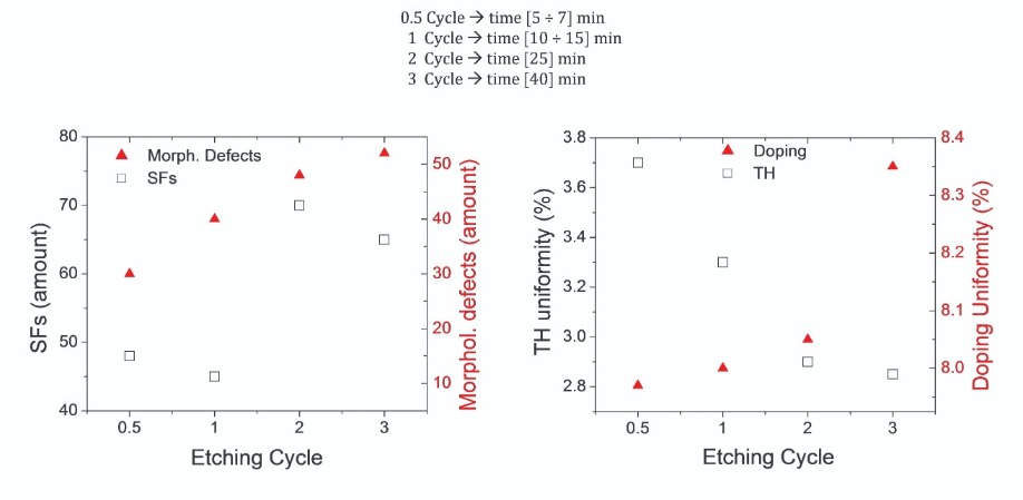
Figure 4. (Left) The number of defects as a function of etching time. (Right) Thickness and doping uniformity as a function of etching time.
Growing the buffer….Once the surface is clean, we begin to grow the epitaxial structure, starting from buffer layer, using nitrogen and aluminium as the n-type and p-type dopants, respectively. The substrate is typically highly doped – the level usually exceeds 1018 atoms/cm3 – so to minimise the doping gap between this and the device layers, the buffer is doped, typically at a concentration between 1015 atoms/cm3 and 1017 atoms/cm3. Additional roles for this layer are to quash the conversion and propagation of substrate defects, known as dislocations, into the epilayer.
An appropriate level of doping must be combined with sufficient epilayer thickness. That’s because thicker layers reduce extended defects, which have a very strong, detrimental effect on device performance (see Figure 5). Unfortunately, this thick layer must be grown slowly during buffer layer growth to prevent the propagation of a kind of dislocation called a basal plane.
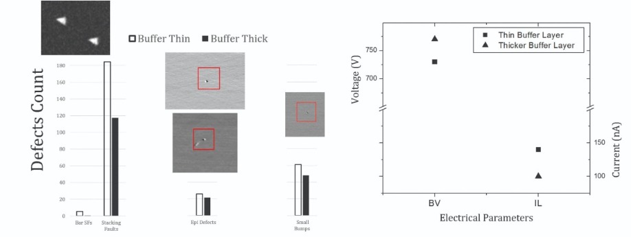
Figure 5. Thicker buffers reduce the defect densities in the epilayer (left), and improve the performance of the MOSFET (right), which benefits from a higher breakdown voltage and a reduction in leakage current.
We have shown that a thicker buffer increases the breakdown voltage of a device, while trimming its leakage current (see Figure 5). Devices could be degraded by the propagation of basal plane dislocations, but these imperfections are avoided by using a sufficiently slow growth rate for the buffer layer.Our latest efforts are directed at studying the impact of the nitrogen flux on the buffer layer. Descending doping ramps during buffer layer growth appear to reduce lattice stress introduced by nitrogen, enabling the growth of a compliant drift layer.
... and the drift layer
It is well known that as epitaxial defects rise, electrical characteristics are compromised. However, to guarantee the functionality of the devices, when it comes to the drift layer, it is essential to combine a very low defect density with high uniformity in thickness and doping. In fact, there are many requirements for the drift layer – in addition to withstanding a high voltage (together with the gate oxide), it has to host many critical manufacturing processes, including post-oxidation annealing, gate oxide fabrication, ion implantation, and thermal annealing.
During the last decade, we have devoted much effort to improving the crystal quality of our epitaxial process. Success has followed and now 95 percent of the area on 6-inch epiwafers is useable, based on calculations using a 2 mm by 2 mm grid. The key to this progress has been the fine tuning of: the growth temperature, which should be uniform within the chamber and higher than 1600 °C; the growth pressure, which should be stable and lower than 100 mbar; and the carbon-to-silicon ratio, which should be within the range 1.1 to 1.3.
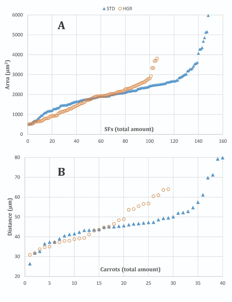
Figure 6. Moving from a standard growth rate process (STD) to a high growth rate process (HGR) reduces stacking faults (A) and carrots (B) in the epilayers.
As well as ensuring uniformity of the growth temperature, pressure, and the carbon-to-silicon ratio, it is imperative that the chemical precursors – for the silicon source, it is typically SiH4 or HCl3Si, and for carbon it tends to be C3H8 or C2H4 – are well purified and widely available for mass production. A high purity is critical, as it holds the key to a high growth rate. For silane chemistry, growth is typically between 5 μm/h and 15 μm/h.Many groups have shown that increasing the growth rate, in tandem with the use of substrates off-cut by 4°, enables a trimming of defect density and improvement in thickness and doping uniformity. By appropriately balancing silicon and carbon precursors and the silicon-to-hydrogen ratio (H2 gas and argon are the typical gas carriers), growth can hit 20 μm/h.
In our laboratories, we have observed these trends, with a strong reduction of defectiveness at higher growth rates. This includes reductions to the density and the size of crystallographic defects, such as stacking faults, and the morphological defect known as a carrot (see figure 6).
To negate the influence of substrate quality on our results, we used material with a very similar crystallographic quality – all substrates came from a small section of one ingot. By taking this precaution, we are confident that it is the higher growth rate that leads to a 10 percent hike in electrical yield, thanks to a reduction of defect density and improvements in thickness and doping uniformity. Evaluating the latter with a figure of merit that equals the difference between the maximum and minimum values, divided by the mean, gives values of less than 5 percent for thickness and below 12 percent for doping.
Cooling down
After growth of our epilayers, our wafers cool down, the gas supply is stopped and the gas line purged. The rate of the cooling is important, as it governs the thermal stress induced within the epilayers. If the stress is significant, it can generate post-growth defects. The hydrogen flow is also a consideration, as this determines the generation of shallow defects, just a few nanometres in size.
We have found that by slowing the cooling rate to less than 25 °C/min, and increasing the flow of hydrogen, we can reduce the thermal stress and increase the time that the surface of the epiwafer is at a higher temperature.
Our approach, which we refer to as a ‘high growth rate cool’, is beneficial. It reduces, by 40 percent, both the number of small defects, defined as having a size of less than 1 μm, and the number of shallow defects, which are just a few nanometres in size. Another feature of our cooling process, which provides an effective cleaning of the surface, is to increase the pressure a little bit.
The combination of the higher growth rate and the slower cool down decreases the density of all major defects (see Figure 7). Thus is encouraging, but our work is not over, as we still need to undertake a
careful inspection of the relationship between epilayer quality and the major growth parameters, including pressure, growth rate, the temperature ramp and the carbon-to-silicon ratio. It is clearly very important to optimise the growth process for every single layer and the cool down. However, this, in itself, cannot guarantee epiwafer quality. That’s because it is also necessary to screen the quality of the substrates, which are formed by slicing ingots and polishing the resulting material.
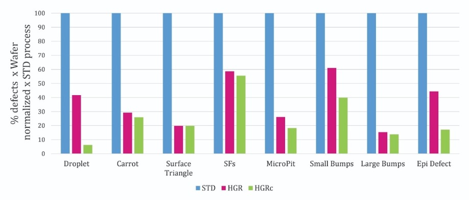
Figure 7. Epilayer crystal quality, judged in terms of defects density, improves by advancing from a standard growth rate process (STD) to a high growth rate process (HGR) that includes a superior cool down (HGRc). Note that the percentage has been normalized to that for the STD process.
The process for making the ingots is improving, but these crystals can still be plagued by dislocations that propagate through the material. These imperfections are problematic, as they drive up epitaxial defect density.We have carried out a statistical survey, evaluating defect densities in thousands of wafers before and after the epitaxial process. This study revealed that when substrates come from an ingot with a nominal dislocation density of less than 3000 per cm2, epilayers have a low defect density even when they are taken close to the seed of the ingot, which is the worst part of the boule. However, if the dislocation density is higher, there is a faster deterioration of epitaxial layer quality, especially for substrates close to the seed (see Figure 8).
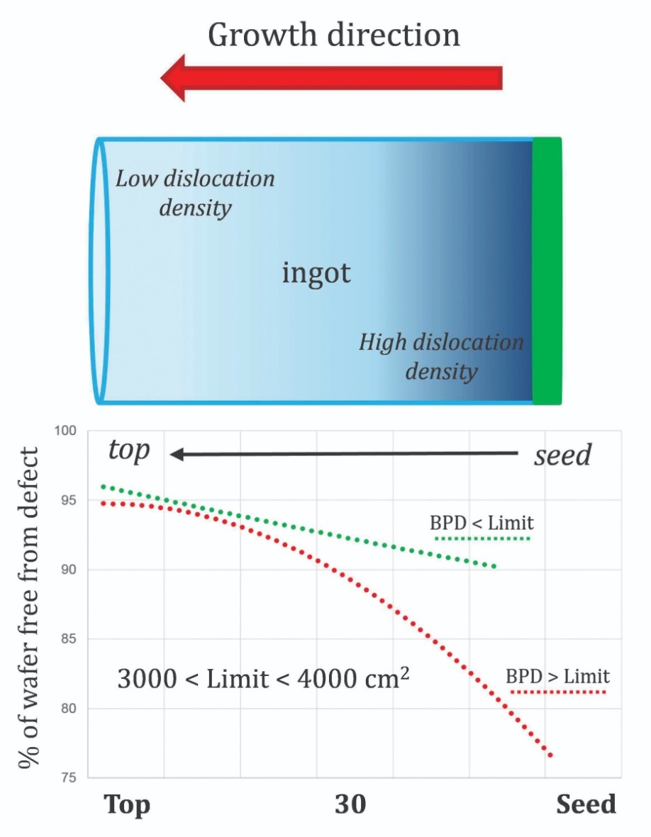
Figure 8. Using wafers with a basal plane dislocation density of less than 3000 per cm2 leads to a significant improvement in epiwafer quality.
Armed with our knowledge of how to optimise the growth and cool down process, and what is required from the substrates, we are well positioned to drive up the quality of SiC material. In turn, this will improve the high-volume manufacture of power devices, and the growth of this industry.Further reading
Y.M. Tairov et al. J. Cryst. Growth 43 209 (1978)
N. Kuroda et al. Extended Abstracts, 19th Conference on Solid State Devices and Materials, Tokyo, Japan, 1987, p. 227 Step controlled VPE growth of SiC single crystals at low temperatures
A. Itoh et al. Silicon Carbide and Related Materials 1993, IOP, p. 59, (1994).
D.J. Larkin et al. Appl. Phys. Lett. 65 1659 (1994)
O. Kordina et al. Silicon Carbide and Related Materials 1993, IOP, p. 41, (1994)
N.Piluso et al. Mater. Science Forum 897 181 (2017)
N.Piluso et al. MRS Advances 1 3673-3678 (2016)
T. Kimoto Jap. J. Appl. Phys 54 040103 (2015)
T. Kimoto et al.. Fundamentals of Silicon Carbide Technology, ISBN: 978-1-118-31352-7 (2014)
F. La Via, Silicon Carbide Epitaxy, ISBN: 978-81-308-0500-9 (2012)


