Loading...
News Article

HexaTech makes Defect-Free 2 inch AlN Substrate

News

Largest known single crystal AlN substrate that is completely free of macroscopic defects

HexaTech, a US supplier of single crystal AlN substrates, has announced the first known demonstration of a defect-free 2 inch diameter AlN substrate.

AlN substrates are used to make long life UV-C LEDs for disinfection applications, deep UV lasers for biological threat detection, and high voltage switching devices for efficient power conversion, and RF components for satellite communications.

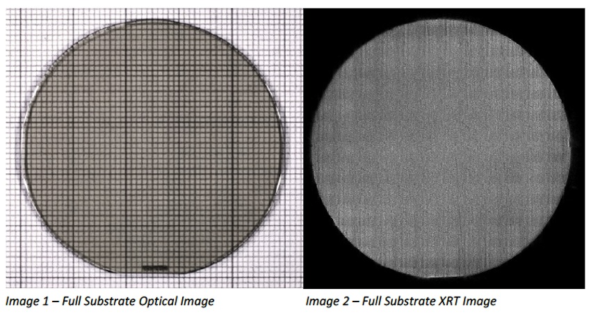
HexaTech co-founder and CTO, Raoul Schlesser commented: “This is the largest known single crystal AlN substrate that is completely free of macroscopic defects, and accomplishes a long-standing goal as part of our 2 inch product development. Full-substrate reflection X-ray topography confirms this achievement, which will support and accelerate commercial production of high quality 2 inch material.”

“Less than a year from our first 2 inch demonstration, reaching this level of perfection is a testament to the efforts of the entire HexaTech team, and highlights our relentless drive to provide our customers the ultimate in AlN substrate performance”, stated HexaTech CEO, John Goehrke. “This capability establishes a new baseline for sustaining our vision of continued diameter expansion and greater market adoption”, he added.

HexaTech’s 2 inch diameter substrates, in addition to 35 mm and 25 mm substrates, are available now with standard lead times.

SiC MOSFETs: Understanding the benefits of plasma nitridation
Wolfspeed reports Q2 results
VueReal secures $40.5m to scale MicroSolid printing
Mitsubishi joins Horizon Europe's FLAGCHIP project
Vishay launches new high voltage SiC diodes
UK team leads diamond-FET breakthrough
GaN adoption at tipping point, says Infineon
BluGlass files tuneable GaN laser patents
QD company Quantum Science expands into new facility
Innoscience files lawsuit against Infineon
Riber revenues up 5% to €41.2m
Forvia Hella to use CoolSiC for next generation charging
Photon Design to exhibit QD simulation tool
Ortel transfers CW laser fabrication to Canada
Luminus adds red and blue multi-mode Lasers
PseudolithIC raises $6M for heterogeneous chiplet tech
Mesa sidewall design improves HV DUV LEDs
IQE revenue to exceed expectations
'Game-changing' VCSEL system targets clinical imaging
German start-up secures finance for SiC processing tech
Macom signs preliminaries for CHIPS Act funding
IQE and Quintessent partner on QD lasers for AI
EU funds perovskite tandems for fuel-free space propulsion
EU to invest €3m in GeSi quantum project
Transforming the current density of AlN Schottky barrier diodes
Turbocharging the GaN MOSFET with a HfO₂ gate
Wolfspeed launches Gen 4 SiC MOSFET technology
Report predicts high growth for UK's North East
Element Six unveils Cu-diamond composite
SemiQ launches hi-rel 1700V SiC MOSFETs
Lynred to exhibit Eyesential SWIR sensor for machine vision
Thorlabs buys VCSEL firm Praevium Research
×
Search the news archive

To close this popup you can press escape or click the close icon.
Logo
x
Logo
×
Register - Step 1

You may choose to subscribe to the Compound Semiconductor Magazine, the Compound Semiconductor Newsletter, or both. You may also request additional information if required, before submitting your application.


Please subscribe me to:


You chose the industry type of "Other"

Please enter the industry that you work in: