
UV light: the key to better 2D devices?
Japanese team shines light on interface properties of graphene and GaN heterojunction
Researchers from the Nagoya Institute of Technology (NITech) in Japan have developed a method to make sure the connections in heterojunction 2D semiconductors are as perfect as possible. The researchers published their results on April 15 in Applied Physics Letters.
Their research involved applying a layer of graphene to GaN. According to Golap Kalita, an associate professor at NITech, understanding GaN heterojunction devices and how to improve them is critical for better device performance.
"Our team found a way to determine the interface properties of the graphene and GaN heterojunction by characterising the device under ultraviolet illumination," Kalita said.
The interface between the graphene and the GaN should be free of impurities, especially ones that gain energy from light. When the researchers shined UV light on the heterojunction device, they found photo-excited electrons (excitons) trapped at the interface and interfering with the transfer of information.
The GaN contains surface-level defects and other imperfections that allow such photo-excited electrons to become trapped at the interface.
"We found that the interface states of graphene and GaN have a significant influence on the junction behaviour and device properties," Kalita said.
One such property is electrical hysteresis - the phenomenon in which electrons get trapped at the interface leading to behavioural shift in the device. The trapping of electrons is extremely sensitive to UV light. It means that once the UV light is shined on the heterojunction, the excited electrons get populated at the interface and remain as trapped, creating large hysteresis window.
However, when the researchers applied a more refined layer of graphene to GaN, they didn't see any the hysteresis effect without light illumination, implying a cleaner match at the interface. But it wasn't perfect - UV illumination instigated the photo-excited electrons into a frenzy behavior due to inherent defects in GaN.
"This finding showed that the graphene/GaN heterojunction interface can be evaluated by the ultraviolet illumination process," Kalita said.
The ability to evaluate the purity of the interface is invaluable in the development of high-performance devices, according to the researchers.
"This study will open up new possibilities to characterise other heterojunction interfaces by an ultraviolet light illumination process," Kalita said. "Ultimately, our goal is to understand interface of various two- and three-dimensional heterostructures to develop novel optoelectronic devices with graphene."
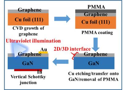
(The diagram above shows the fabrication process of a vertical Schottky junction with monolayer graphene on free-standing GaN.)
'Ultraviolet light induced electrical hysteresis effect in graphene-GaN heterojunction' by Ajinkya K. Ranade et al; Appl. Phys. Lett. 114, 151102 (2019)


