
EVG starts construction of €30 million cleanroom project
Large cleanroom in St. Florian am Inn creates additional development, demo and pilot production capacity
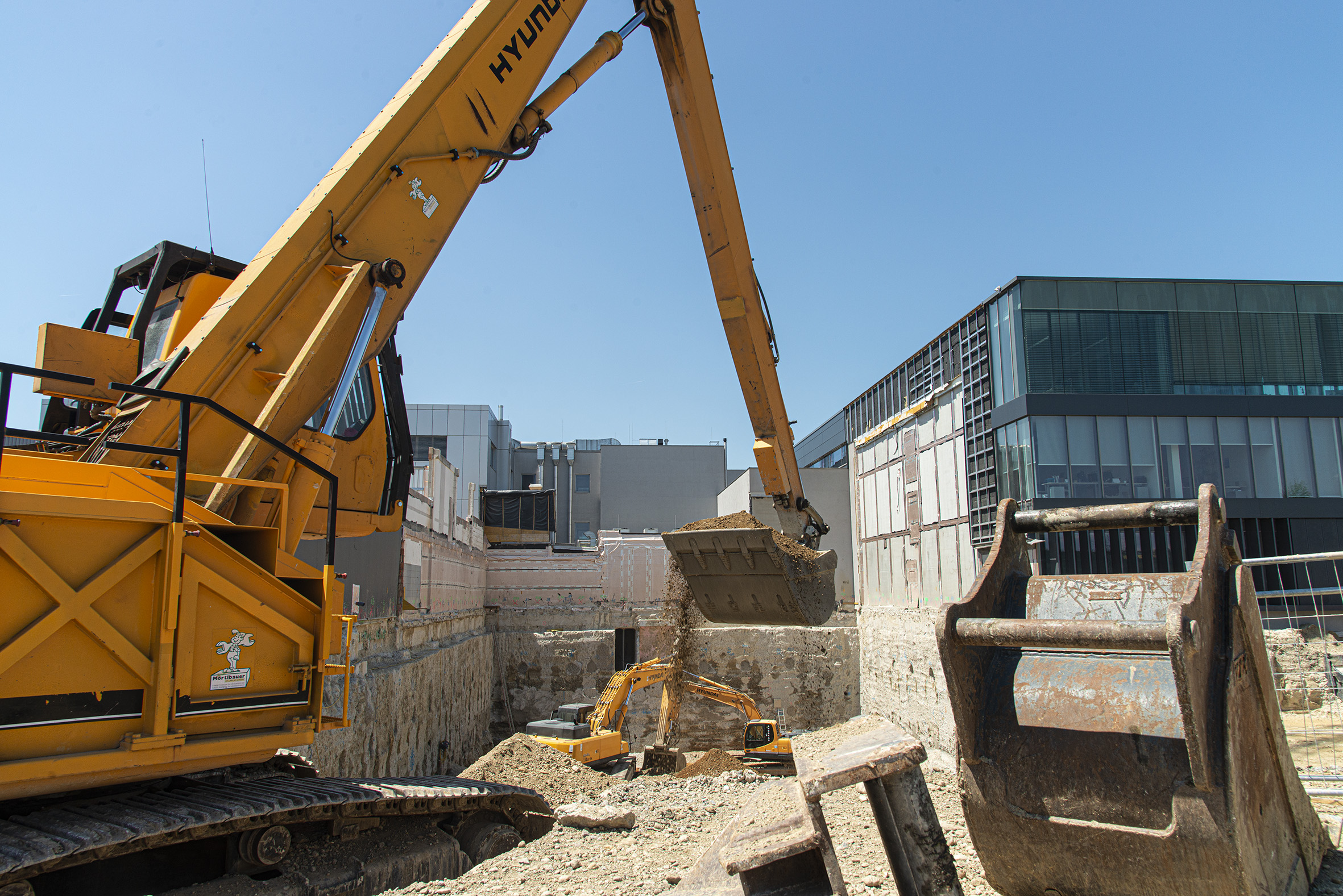
EV Group (EVG), a supplier of wafer bonding and lithography equipment for the MEMS, nanotechnology and semiconductors, has announced that it has begun construction on another extensive building project at its corporate headquarters in St. Florian am Inn, Austria. With an investment of €30 million, the new Cleanroom V building will create additional capacity for product and process development, equipment demonstrations for existing and potential customers, feasibility studies as well as prototyping and pilot production.
The groundwork for the new building was recently finished and includes footings that reach up to 14 metres deep into the ground. Once the new cleanroom is completed, it will host equipment, such as EVG's lithography systems, wafer bonders and metrology systems, which operate with micro- and nanometer accuracies. The contaminant-free conditions of EVG's cleanrooms at its headquarters, as well as its subsidiaries in America and Asia, are comparable to those in the fabs of EVG's worldwide high-tech industry customers.
"Just this past April, EV Group celebrated the opening of our new Manufacturing III facility with our employees, which itself provides 1,800 square meters of additional production floor space for the final assembly of our equipment," stated Werner Thallner, executive operations and financial director at EV Group. "In the meantime, the construction crews already started to work at the other end of our campus on this new building, which will add even more capacity to support our business growth. With the investment in expanding our cleanroom capacity, we continue to demonstrate our local commitment to Austria, as well as our global commitment to our worldwide customers."
Markus Wimplinger, EVG's corporate technology development and IP director, added: "Our engineers develop and optimize wafer processes for our equipment to fulfill individual production requirements, often in close cooperation with our customers. This new building will open completely new opportunities to the EVG technology teams."
The new Cleanroom V building will provide approximately 620 square meters of additional cleanroom floor space - nearly doubling the cleanroom capacity at EVG's headquarters. In total, the new building will encompass a floor space of about 4,400 square meters. The construction work is set to be completed by the middle of next year.


