
Understanding SiC defects
Swiss physicists show how SiC defects are generated during oxidation
Modern power electronics must be able to handle large currents and high voltages. SiC offers significant physical and chemical advantages over silicon in this respect. But the advantages of h higher heat resistance, and better energy efficiency, are compromised by defects at the interface between SiC and the insulating material silicon dioxide.
Now physicists of the University of Basel, the Paul Scherrer Institute, and ABB have now explained the nature of these defects in a paper in Applied Physics Letters.
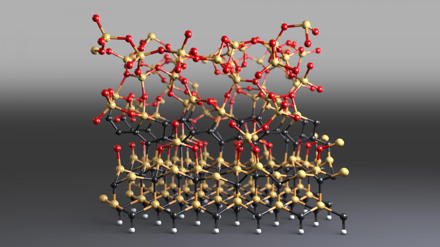
Thomas Jung and colleagues at the Swiss Nanoscience Institute and Department of Physics from the University of Basel and the Paul Scherrer Institute used atomic force microscope analysis and Raman spectroscopy to show that the defects (tiny, irregular clusters of carbon rings bound in the crystal lattice) are generated in the vicinity of the interface by the oxidation process.
The interfering carbon clusters, which are only a few nanometers in size, are formed during the oxidation process of SiC to silicon dioxide under high temperatures. "If we change certain parameters during oxidation, we can influence the occurrence of the defects," says doctoral student Dipanwita Dutta. For example, a nitrous oxide atmosphere in the heating process leads to significantly fewer carbon clusters.
The experimental results were confirmed by the team led by Stefan Gödecker at the Department of Physics and Swiss Nanoscience Institute from the University of Basel. Computer simulations confirmed the structural and chemical changes induced by graphitic carbon atoms as observed experimentally. Beyond experiments, atomistic insight has been gained in the generation of the defects and their impact on the electron flow in the semiconductor material.
Better use of electricity
"Our studies provide important insight to drive the onward development of field-effect transistors based on SiC. Therefore we expect to provide a significant contribution to the more effective use of electrical power," comments Jung. The work was initiated as part of the Nano Argovia program for applied research projects.
'Evidence for carbon clusters present near thermal gate oxides affecting the electronic band structure in SiC-MOSFET' by D. Dutta et al; Applied Physics Letters, 2019 DOI: 10.1063/1.5112779


