Perovskite stability: new insights

University of Groningen teams uses X-rays to reveal in situ crystal growth of lead-free perovskite solar panel materials
Around a decade ago, scientists discovered taht metal-halide perovskite could convert light into electricity. The first perovskites solar cells perovskites contained lead, which is toxic. Alternative tin-based perovskites had the downside of being unstable.
In recent years, scientists at the University of Groningen have shown how adding 2D layers instead of 3D crystals increased the stability on tin-based perovskite cells; however, this was at the expense of efficiency. Now, they have 'watched' how thin films of tin-based perovskite crystals grow. The results of this new study were published in the journal Advanced Functional Materials on 31 March.
The team have discovered that in mixtures of 3D and 2D perovskites, the 2D component helps to orient the 3D-like crystals but, at the same time, the 2D perovskite forms an insulating layer that is in contact with the substrate. Their latest research suggests that by breaking up this insulating layer, it should be possible to create more efficient and stable tin-based perovskite solar panels.
Maria Loi and Giuseppe Portale investigated what happens during the tin-perovskite film formation using an X-ray diffraction technique, that allowed them to study the rapid formation of thin films in real-time during spin-coating from solution.
On a laboratory scale, the perovskite films are generally made by spin coating, a process in which a precursor solution is delivered onto a fast-spinning substrate. Crystals grow as the solvent evaporates. At the beamline BM26B-DUBBLE at the European Synchrotron Radiation Facility (ESRF) in Grenoble, France, Portale investigated what happens during the tin-perovskite film formation.
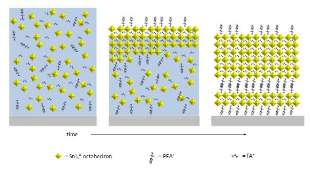
"Our initial idea, which was based on ex situ investigations, was that the oriented crystals grow from the substrate surface upwards," Portale explains. However, the in situ results showed the opposite: crystals start to grow at the air/solution interface. During his experiments, he used 3D FASnI3 with the addition of different amounts of the 2D PEASnI4. In the pure 3D perovskite, crystals started to form at the surface but also in the bulk of the solution. However, adding a small amount of the 2D material suppressed bulk crystallisation and the crystals only grew from the interface.
"PEA molecules play an active role in the precursor solution of the perovskites, stabilising the growth of oriented 3D-like crystals through coordination at the crystal's edges. Moreover, PEA molecules prevent nucleation in the bulk phase, so crystal growth only takes place at the air/solvent interface," Portale explains. The resulting films are composed of aligned 3D-like perovskite crystals and a minimal amount of 2D-like perovskite, located at the bottom of the film. The addition of low concentrations of the 2D material produces a stable and efficient photovoltaic material, while the efficiency drops dramatically at high concentrations of this 2D material.
"The 2D-like perovskite is located at the substrate/film interface. Increasing the content of the 2D material to above a certain amount causes the formation of an extended 2D-like organic layer that acts as an insulator, with detrimental effect for the device's efficiency,"
The conclusion of the study is that the formation of this insulating layer must be prevented to achieve a highly efficient and stable tin-based perovskite. The next step is to realise this, for example by playing with solvents, temperature or specific perovskite/substrate interactions that can break up the formation of this thick insulating layer.
The picture above shows mechanism of crystallisation from the DMF/DMSO solution during drying for the 2D/3D perovskite films.
'Mechanism of Crystal Formation in Ruddlesden–Popper Sn‐Based Perovskites' by Jingjin Dong et al; Advanced Functional Materials, 31 March 2020


