Hybrid growth promises better performing laser diodes

Adding tunnel junctions by remote-plasma CVD will lead to more-powerful, more-efficient GaN lasers
BY JOSH BROWN, BRAD SISKAVICH AND IAN MANN FROM BLUGLASS
THE DEVELOPMENT of high-brightness GaN-based lasers is opening the door to new and exciting applications. This class of lasers is starting to be used for industrial welding, biotech-flow cytometry, displays, and general and automotive lighting. Sales in these sectors are tipped to rocket over the next few years.
To turn the promise of significant commercial success into reality, there has to be an improvement in the optical performance and the energy conversion of these lasers. Efforts need to be directed at extending their spectral range, increasing their power, and boosting their efficiency and brightness.
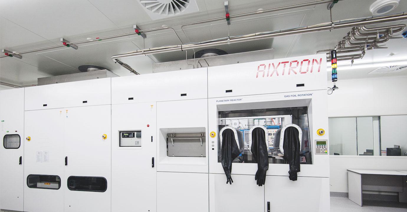
At BluGlass Limited of Silverwater, Australia, we have a novel technology for addressing many of these challenges – low temperature, ammonia-free GaN deposition. It is a supplementary growth method that is based on remote-plasma CVD and offers laser diode manufacturers performance and cost advantages over the traditional MOCVD-only process. To ensure that this technology has commercial impact, last October we launched a laser diode business for exploiting our unique remote-plasma CVD growth platform for the manufacture of high-brightness GaN lasers.
-rev-p2rmr4.jpg)
-7isss3.jpg)
Figure 1. (a) (top) Structure of standard laser diode without a tunnel junction and (b) (bottom) normalised optical mode and refractive index profile.
During the growth of laser diodes, remote-plasma CVD offers an ‘active-as-grown’ buried p-GaN technology. It enables the production of high-performance tunnel junctions, without the need for post-growth annealing for the activation of the magnesium acceptors.Originally, we developed our ‘active-as-grown’ tunnel junctions for use in LEDs, but now they are being deployed in unique laser diode designs. Our hope is that this technology will help to bridge the substantial gap between the performance of these two optoelectronic devices – in state-of-the-art GaN-based laser diodes, conversion efficiency is still only around 40 percent, compared with nearly 90 percent in GaN-based LEDs.
The problems of p-doping
There are many factors behind this low conversion efficiency for laser diodes. Quite a few relate to the high activation energy of the magnesium acceptor in p-type, magnesium-doped layers of GaN and AlGaN. Due to an activation energy of around 170 meV, typically just 1 percent of the magnesium atoms contribute to the free-hole concentration. Consequently, to make viable devices, magnesium doping levels in p-type layers have to be cranked up – they are often up to 100 times higher than the silicon doping in n-type layers.
Putting so much magnesium in the epilayers is not ideal. It leads to low hole mobilities, high resistivities and a high optical loss – and it ultimately drags down the conversion efficiency of the laser diodes. Optical losses occur in the p-side, and are most acute in the p-AlGaN cladding layer. To ensure confinement of the optical mode within active region and waveguide layers, this cladding has to have a relatively low refractive index. However, this cannot prevent a fraction of the mode overlapping the p-doped, AlGaN layer. As there are high levels of magnesium in this layer, the absorption coefficient is very high – it typically exceeds more than 100 cm-1 – and it contributes a significant fraction to the total optical loss in this class of laser.
The p-type resistive loss comes from a combination of the series resistance in the p-AlGaN cladding and the high p-side contact resistance. Together, this can account for up to 50 percent of the power consumption, when this device is driven at operating current densities well above the lasing threshold. These losses manifest themselves in the form of Joule heating.
-rev-cbk3kk.jpg)

Figure 2. (a) (above) Tunnel-junction laser diode structure and (b) (bottom) total optical loss as function of thickness and silicon doping levels in the n++ layer of the tunnel junction.
The tremendous tunnel-junctionWe are able to address the optical and resistive losses in GaN-based laser diodes with a technology that sidesteps the problems associated with p-doping of GaN. We draw on our previous success, which involves using remote-plasma CVD to grow active-as-grown tunnel junctions for cascade LEDs that address efficiency droop. Now we are applying the technology and the techniques to laser diodes. In these devices, we replace the p-type metal ohmic contact with a lower-resistivity n-type ohmic contact, enabled by a GaN-based tunnel-junction that provides conversion between n-type and p-type regions. This design eliminates the high p-side contact resistance that plagues conventional laser diodes.
With this approach, optical and resistive losses in the p-AlGaN cladding layer remain. To address this, the tunnel junction must be positioned deeper within the structure – it needs to be moved to within or even below the p-AlGaN cladding layer. Doing this enables the highly resistive p-AlGaN cladding layer to be replaced with much lower resistance n-AlGaN. In turn, this reduces the optical absorption coefficient, due to the lower silicon-doping requirements.
Great care is needed in designing the tunnel-junction and selecting its location. It must be positioned so that any increase in optical losses associated with its addition is offset by a comparable reduction in losses that come from the replacement of p-type layers with those that are n-type. In addition, it is crucial to ensure that the resistance in the tunnel-junction is low enough to be offset by the reduction in series and contact resistance. It is only by meeting both of these criteria that the tunnel-junction laser diode can offer a viable solution to increasing the conversion efficiency of GaN-based lasers.
We have investigated how the structure and placement of the tunnel junction impacts the optical losses in laser diodes. To do this, we have simulated various laser diode structures (see Figure 1 (a) for details of the design and the absorption coefficients that have been used). This has included calculations of the refractive index profile and distribution of the optical mode. For these simulations, values for the absorption coefficients of the n-type and p-type layers have been based on benchmark doping levels. Results show that a large proportion of the total optical loss – it is more than 80 percent – is associated with the p-side of the device (see Figure 1 (b)). Losses are high in the electron-blocking layer, the p-type waveguide, and the p-cladding layers.
With this benchmark in place, we repeated the simulation for a laser diode that incorporates a tunnel-junction (see Figure 2(a) for details of the design). This has the same base structure, but has: a tunnel-junction at the top of the p-type waveguide; and rather than a p-type AlGaN cladding and a heavily p-type doped contact layer, an n-type AlGaN cladding and a heavily doped n-type contact layer.

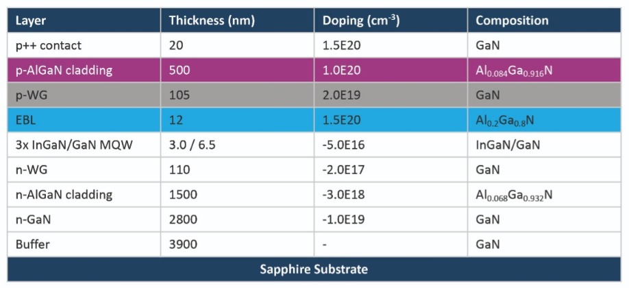
Figure 3. A standard MOCVD laser diode on a sapphire structure.
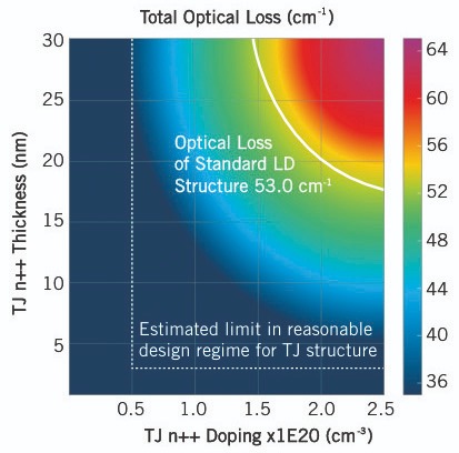
One of our simulations considered the total optical loss as a function of layer thickness and silicon doping level in the heavily-doped n-type layer of the tunnel junction (see Figure 2 (b)). As expected, greater losses come from thicker, more heavily-doped junctions. Included in this plot is a white contour line, which corresponds to the total optical loss of the standard laser diode, which does not have a tunnel junction. If devices with a tunnel junction are to be a success, then they will have to have a total optical loss that is less than this.The simulation provides an estimate of the upper limit for the doping and the thickness that can be tolerated within the heavily-doped n-type layer of the tunnel junction to ensure a net overall reduction in optical loss for this type of laser. In this figure, the white dashed line offers an estimate of the lower limit for thickness and doping values in the heavily doped n-type layer to realise reasonable tunnelling behaviour.

The inside of an remote-plasma CVD chamber during growth, showing active nitrogen.
Working devicesTo put these simulations to the test, we have fabricated laser diodes on sapphire substrates. Using MOCVD, we have produced lasers with a structure that is similar to that detailed in Figure 1, and is shown in Figure 3.
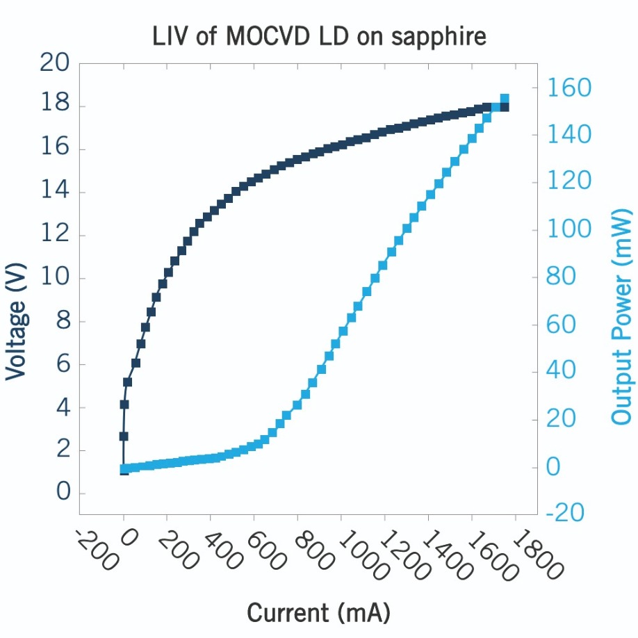
Through a collaboration with researchers at the University of New Mexico, we have been able to process our epiwafers into ridge-waveguide laser diodes. Pulsed measurements reveal the relationship between the output of this device, the applied voltage and the drive current (see Figure 4). Emitting at 397 nm, these lasers produce an output power from one facet of up to 155 mW. The voltage required to run these devices could be improved with further optimisation of the p-AlGaN cladding layer.

Figure 4. Light-current-voltage measurements of an MOCVD-grown laser diode on a sapphire substrate.
Our next step has involved integrating the tunnel-junction grown by remote-plasma CVD within these lasers diodes, and seeing if this improves device performance through reductions in optical loss and device resistance. We were keen to find out if tunnel junctions could be grown with a low enough doping and/or thickness in the heavily-doped n-type layer to yield a net reduction in optical loss compared to our reference. We also wanted to discover whether the addition of the tunnel junction produced only a small increase in drive voltage.To optimise our tunnel junctions for laser diodes, we began by growing them by remote-plasma CVD on commercially sourced blue LEDs. For the current spreading layer, we used a top n-doped GaN layer, rather than indium tin oxide (see Figure 5 (a) for a diagram of the device). Measurements on a portfolio of processed and packaged devices with different forms of tunnel junctions show that, in general, tunnel junctions with a higher level of doping produce a smaller voltage drop during operation (see Figure 6 (a)). Note that the light output from all devices is similar.
-rev-6r6h4u.jpg)
-rev-oqknc3.jpg)
Figure 5. (a) Hybrid MOCVD/remote-plasma CVD tunnel-junction structure and (b) a table of n++ parameters used to optimise the tunnel junction for laser diode applications. The delta Vf in the last column refers to the difference in forward voltage, Vf, of the tunnel-junction LED compared with the reference LED using ITO.
We have simulated the total optical loss for lasers with all of these forms of tunnel junction (see Figure 6 (c)). Encouragingly, the laser with the tunnel junction that has the smallest increase in drive voltage has a total optical loss of 47.9 cm-1 – that’s just below the contour line that represents the total optical loss of the standard laser diode without a tunnel junction. This is a crucial finding, as it reveals that laser diodes that have a tunnel junction grown by remote-plasma CVD and are optimised to have the lowest increase in the drive voltage can yield a net reduction in total optical loss. This paves the way to improved devices, which feature a reduced series and contact resistance, due to the replacement of p-type cladding and p-type contact layers with n-type cladding and n-type contact layers.Building on this discovery and our demonstration of lasing behaviour from laser diodes that do not contain tunnel junctions and are formed by MOCVD, we have recently gone on to grow lasers with tunnel junctions by combining MOCVD and remote-plasma CVD. These devices, grown completely within our facilities, have a foundation of c-plane free-standing GaN. On this we grow layers up to the heavily p-type tunnel junction layer by MOCVD, before adding the remaining layers by remote-plasma CVD (see Figure 7 (a) for a diagram of this device).
-53a44t.jpg)
-5tpn9g.jpg)
-rev-zgqrov.jpg)
Figure 6. (a) Tunnel junction LED delta Vf compared to a reference LED with ITO for tunnel junctions with n++ doping of 2.4 x 1020 cm-3 and different n++ thickness and (b) n++ thickness of 13 nm and different doping levels. (c) Location of the simulated optical loss for tunnel junction laser diode with the same tunnel junction structure as tested on the LEDs.
Collaborators at the University of New Mexico have processed our structures into ridge-guide lasers. Testing of these devices is in its infancy. We do have results of current-voltage characteristics obtained when driving the laser in pulsed mode. Further development is required to fully characterise the optical output of these devices, but initial results are encouraging, with lasers exhibiting normal diode behaviour without breakdown at up to 20.5 kAcm-2 (see Figure 7 b).Unlocking opportunities
Efforts at developing our tunnel-junction laser diode technology will continue, with the goal of unleashing the potential of new GaN laser diode designs across multiple wavelengths and power levels, so that this class of device can serve a wide variety of applications. We are off to a good start, as our initial results demonstrate the promise of remote-plasma CVD tunnel junctions for realising p-AlGaN-free laser diode structures that offer improved device performance, thanks to reductions in optical loss and series and contact resistance.
-rev-e61d03.jpg)
-r3uqis.jpg)
Figure 7. (a) Tunnel junction laser diode structure and (b) light-current-voltage data from a processed laser diode.
Note that we are not alone in championing the benefits of tunnel-junctions in laser diodes. Joachim Piprek, founder and president of NUSOD, has calculated that conversion efficiency could increase from 30 percent to 60 percent with the addition of a tunnel junction. However, he reported that the potential improvements were limited, due to the additional optical loss associated with the highly-doped layers in the tunnel junction.As we have shown, this limitation can be overcome. By suitably controlling the doping and thickness in the n++ layer of the tunnel junction, we can produce low-loss tunnel-junction laser structures with a net reduction in total optical loss compared with standard lasers. A reduction in both Joule heating losses and optical losses is promised, leading to higher conversion efficiencies in GaN laser diodes. That’s the target for us, as we continue to improve laser diode performance with bespoke solutions for existing customers, and start to work with new laser diode developers, so that the market will benefit from greater availability of high-brightness devices that incorporate tunnel junctions grown by remote-plasma CVD.


