US scientists detect X-rays with perovskite

Detector is 100 times more sensitive than conventional, silicon-based X-ray detectors
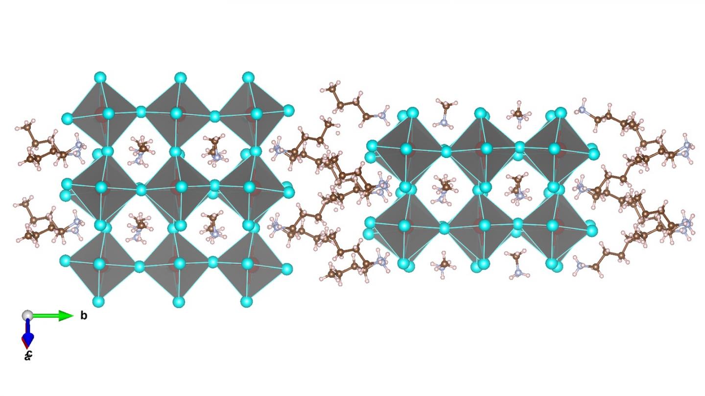
Scientists at the US Department of Energy's (DOE) Argonne National Laboratory and Los Alamos National Laboratory have identified a new class of X-ray detectors based on layered perovskites. The detector with the new material is 100 times more sensitive than conventional, silicon-based X-ray detectors. Their paper 'Highly sensitive and robust thin film X-ray detector using 2D layered perovskite diodes' was published in Science Advances on April 10th 2020.
"This new material for detecting X-rays could soon find its way into a variety of different everyday environments, from the doctor's office to airport security lines to research labs," said Argonne X-ray physicist Joseph Strzalka, who helped to characterise the perovskite material at Argonne's Advanced Photon Source (APS), a DOE Office of Science User Facility.
The perovskite materials work because they are deposited as a sprayed-on thin film, a production method that helps to reduce cost compared to having to grow a large silicon single crystal.
The new perovskite detectors can also detect X-rays over a broad energy range, especially at higher energies. This is because the perovskite contains heavy elements, such as lead and iodine, which tend to absorb these X-rays more readily than silicon. The potential even exists for the perovskite technology to be used as a gamma-ray detector, provided the films are made a little bit thicker and a small external voltage is applied.
"The perovskite material at the heart of our detector prototype can be produced with low-cost solution process fabrication techniques," said Hsinhan (Dave) Tsai, an Oppenheimer postdoctoral fellow at Los Alamos National Laboratory. "The result is a cost-effective, highly sensitive and self-powered detector that could radically improve existing X-ray detectors, and potentially lead to a host of unforeseen applications."
The development and analysis of the perovskite material was a close collaboration between Argonne APS (beamline 8-ID-E) and a Los Alamos team lead by device physicist Wanyi Nie. The material and thin film was created at Los Alamos and brought to Argonne to perform grazing incidence wide-angle X-ray scattering, which gives information about the crystallinity of the thin film. According to Strzalka, the technique shows how the crystal is oriented in the thin film, which relates to the performance of the detector.
Strzalka and Nie were also interested in how the charge transport properties of the film related to the crystal structure and temperature. By using a special stage that allowed the researchers to change the temperature of the sample and make electrical contacts during the measurement, they were able to understand the current generation and transport processes induced in the sample by the X-ray exposure.
"Our instrument at the beamline provides a versatile platform for different kinds of in-situ measurements, including keeping the sample in a vacuum environment while maintaining its temperature and also performing charge transport measurements," Strzalka said.
According to Strzalka, perovskites may continue to offer important breakthroughs. "The perovskite area is really hot right now, and users come to us to say 'can we do this and can we do that,' and it's really pushing us to develop our capabilities," he said.
The research was funded by the Los Alamos National Laboratory's Laboratory Directed Research and Development (LDRD) funding and DOE's Office of Science.


