
Designing tomorrow’s VCSELs

Dedicated, carefully constructed models allow VCSEL designers to evaluate the consequences of temperature on the gain, output power and spatial profile of the device
BY DOMINIC GALLAGHER FROM PHOTON DESIGN AND Sam Shutts FROM THE University of Cardiff
One of the biggest selling devices within today’s compound semiconductor portfolio is the vertical cavity, surface-emitting laser (VCSEL). Its meteoric rise is evident in a recent announcement by Trumpf, boasting that it has shipped two billion of them. Many of these devices will have been deployed in mobile phones, such as those made by Apple, which uses hundreds in its Face-ID function.
Manufacturing VCSELs involves a series of steps that differ from those used for the production of conventional, edge-emitter lasers. Making the latter involves dicing a processed semiconductor wafer into small chips. Light is emitted out of their edge, creating a horizontal lasing cavity.
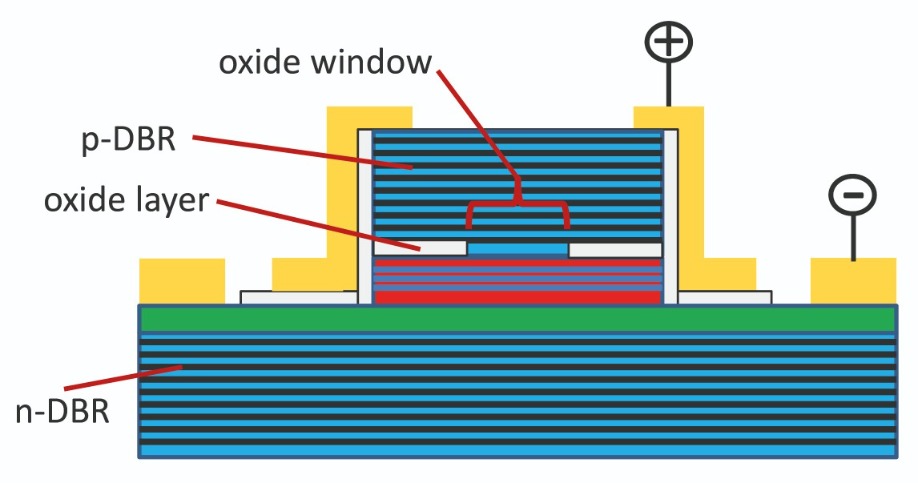
Figure 1. A typical VCSEL structure contains an active layer sandwiched between a pair of mirrors: an n-DBR (distributed Bragg reflector) and p-DBR. Current makes its way through the mirrors to the active layer.
For the VCSEL, the production process is far more challenging. To define the vertical cavity, very high reflectivity mirrors are formed above and below the semiconductor junction. Fortunately, the rewards for this additional complexity are great – the device that results is small in size, has a low threshold current and provides a cheap optical connection.For designers, the VCSEL presents a number of challenges. Like all forms of laser, it features a gain medium surrounded by a pair of mirrors. As light bounces between them, criss-crossing the gain medium, optical losses occur on each round trip. These losses must be compensated by optical gain. That’s a relatively easy requirement to fulfil in a typical edge-emitting laser diode with a 200 μm waveguide that amplifies the lasing light – a mirror with a 50 percent reflectivity is sufficient to double optical intensity in a single pass. In comparison, a VCSEL must achieve the same with a gain region of just 0.1 μm. This demands mirrors that reflect well over 99 percent of the light. While fulfilling this criterion, the light absorbed or scattered inside the cavity must be minimised. If just 0.5 percent of the light is lost in this manner, that still enough to severely impair device efficiency.
To produce mirrors with such a high reflectivity, engineers grow a stack of alternating high and low refractive index layers (see Figure 1). To help them with this task, they want to turn to modelling – but great care is needed to ensure that the results are valid. Modelling VCSELs is far from easy, as the level of accuracy that is acceptable in most devices – normally a few percent is fine – simply will not do. If conventional modelling were to use a mirror reflection loss of around 1 percent, and a similar value for the transmission loss, it would deliver a nonsensical result.
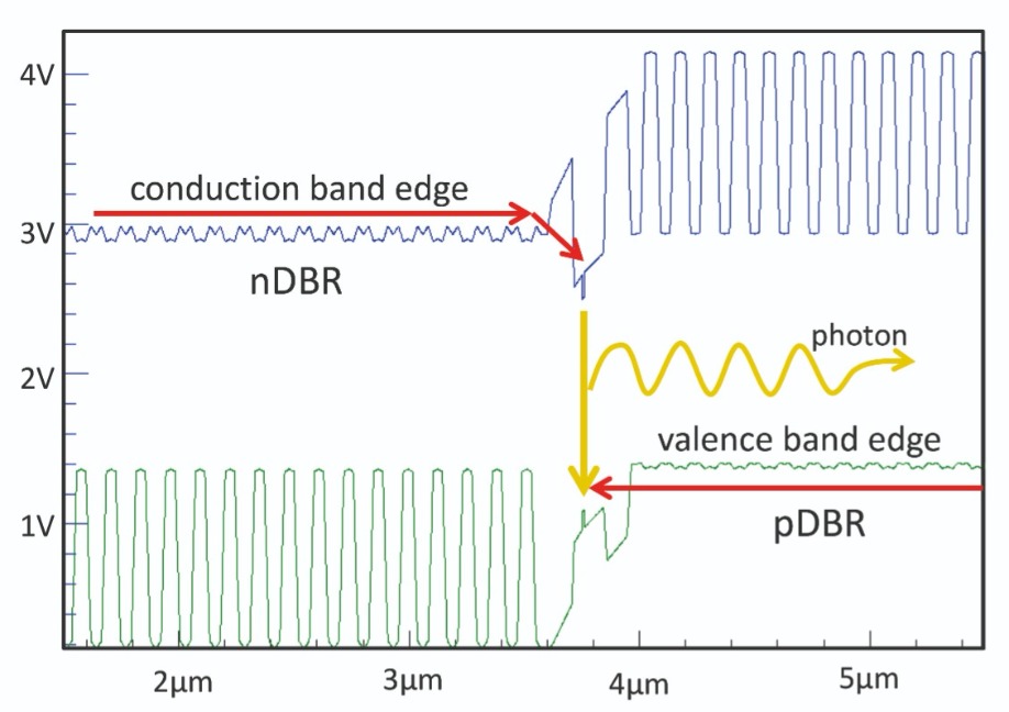
Figure 2. Band edge diagram through the axis of a VCSEL.
Complicating matters, simulations of the electronic behaviour of a VCSEL presents challenges that are not faced by any silicon semiconductor simulator. One of the biggest is that the many interfaces in the mirror play havoc with the flow of electrons and holes (see Figure 2 for an electronic band diagram of a VCSEL).Clearly, what’s needed to support the designers of VCSELs is a dedicated, reliable, multi-disciplinary simulation tool. Serving this need is Harold/VCSEL, a tool developed by Photon Design, a company based in the UK that one of us works for. This simulation software, which is capable of modelling most of the subtleties of the optical and electronic properties that are at play in a modern VCSEL, has been used by our other co-author, an academic at Cardiff University, during the production of devices that can serve in a real-life application – atomic clocks.
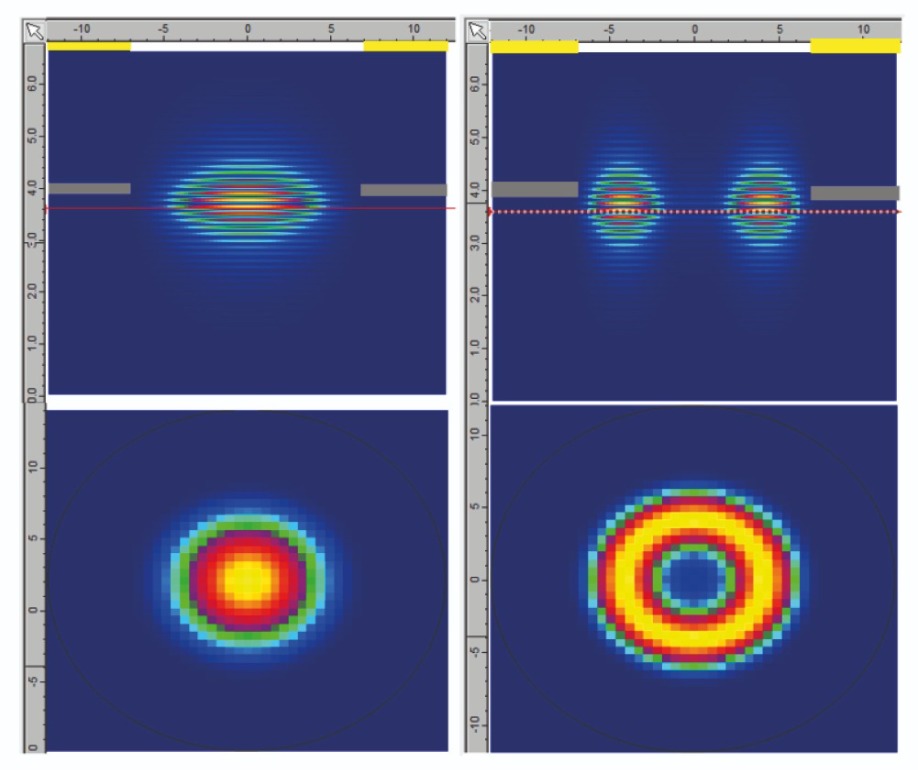
Figure 3. The cavity modes of a VCSEL – top row: side view and bottom row: plan view.
Designing the deviceTo sustain lasing in a VCSEL, the mirrors of this device must have reflectivities of at least 99.5 percent. Helping to accomplish this are the Distributed Bragg Reflectors (DBRs) – stacks of layers with different refractive indices that produce periodic reflectivity. But these reflectors, on their own, are insufficient – the VCSEL must also confine the light laterally. In particular, there is a need to keep the cavity mode away from the walls of the VCSEL, where losses increase.
The common way to accomplish this is to include an ‘oxide aperture’. This is created by oxidising one or two epitaxial layers inwards from the walls of the device to form a light-guiding ring with a lower refractive index (see Figure 3 for an illustration of cavity modes). Using this design, current is injected into the laser via a ring contact on the top surface.
Carriers flow through the DBR to get to the active region (see Figure 1). Unfortunately, this modus operandi is exactly what you don’t want, with the current highest at the tip of the oxide window, and lowest at the peak of the fundamental mode, which occurs in the middle of the VCSEL axis (see Figure 4). When this happens, higher order modes are favoured.
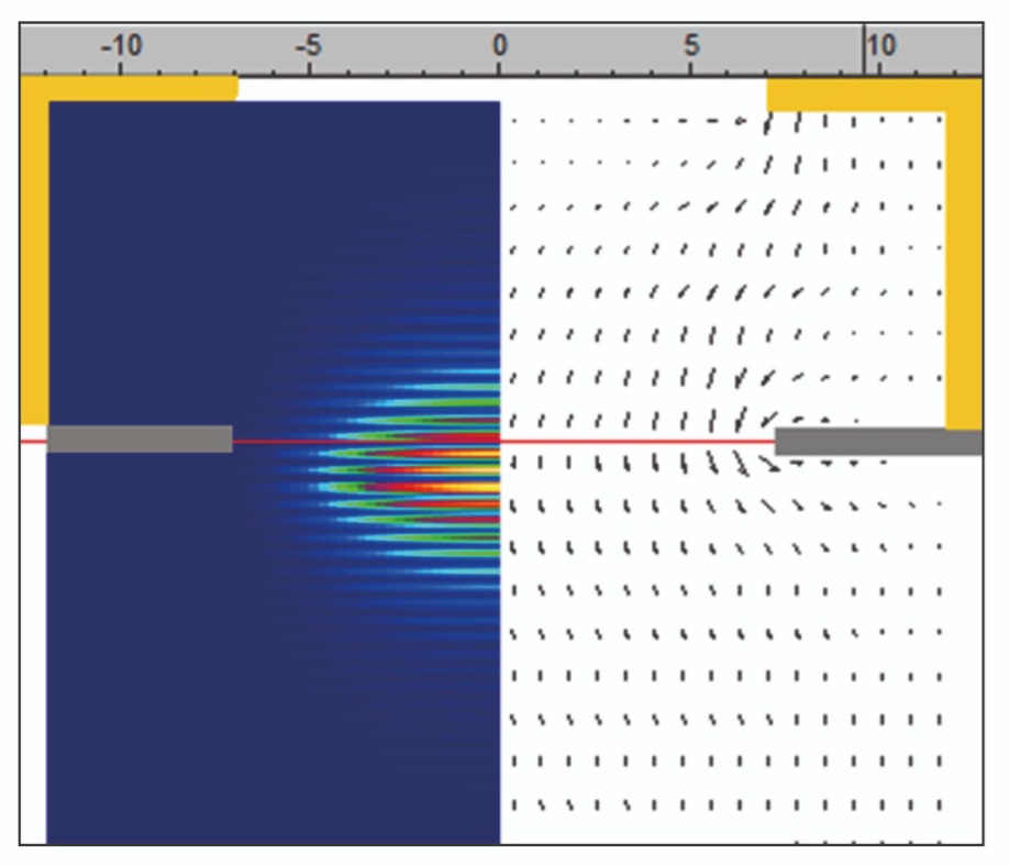
Figure 4. Cross-section of a top-contacted VCSEL, showing the computed mode on the left half and the current flow on the right half.
For VCSELs operating at longer wavelengths – for example, those emitting at 1.3 μm and beyond – it is particularly problematic to create a good DBR stack, due to a reduction in the refractive index contrast, which has to be addressed by adding more layers. Injecting carriers through a thick p-type DBR is not easy, so some designs involve injection from the side (see Figure 5). With issues related to conductivity avoided, the top DBR can now be optimised for its optical properties. But the price to pay is a reduction in current flowing into the centre of the active layer – and that’s precisely where it is needed most to support the fundamental cavity mode.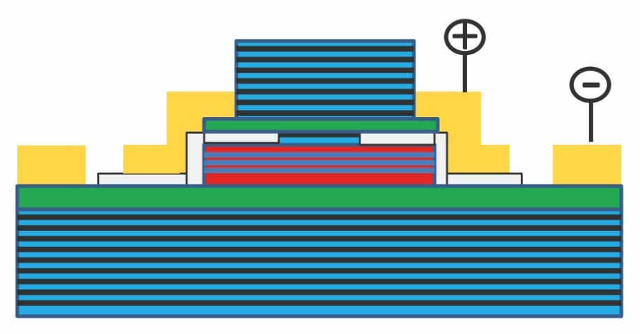
Figure 5. A side-injection VCSEL, with current bypassing the top DBR stack.
The need to keep coolThe output power of the VCSEL is primarily limited by the heat generated within this chip. It comes from a combination of electrical resistance, non-radiative charge recombination, absorption of photons and, particularly, a process known as Auger recombination (see Figure 6).
One of the contributors to the electrical resistance is the interfaces in the DBR mirrors. Add more layers, and this resistance increases.
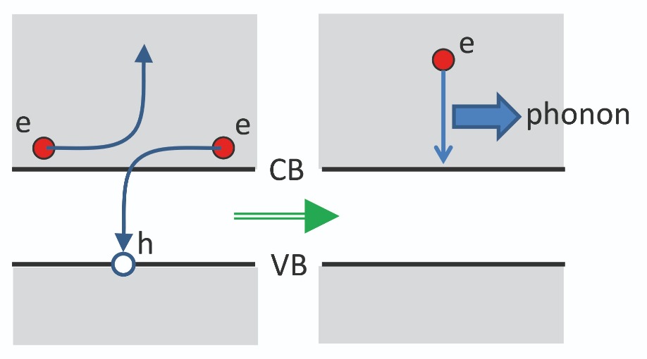
Figure 6. One of the significant loss mechanisms in the VCSEL is Auger recombination. When two electrons in the conduction band collide, this can cause one to recombine with a hole, while the second is excited further up the conduction band. The result is that the excited electron is converted to heat. This problem gets worse at longer wavelengths.
Our simulations also show that as the current through the device increases, its temperature rises rapidly (see Figure 7). This causes two adverse effects – a reduction in gain and an increase in Auger recombination – and both of them lead to even more heating. As a result, as the current through a VCSEL is cranked up its output power rises, peaks, and then decreases.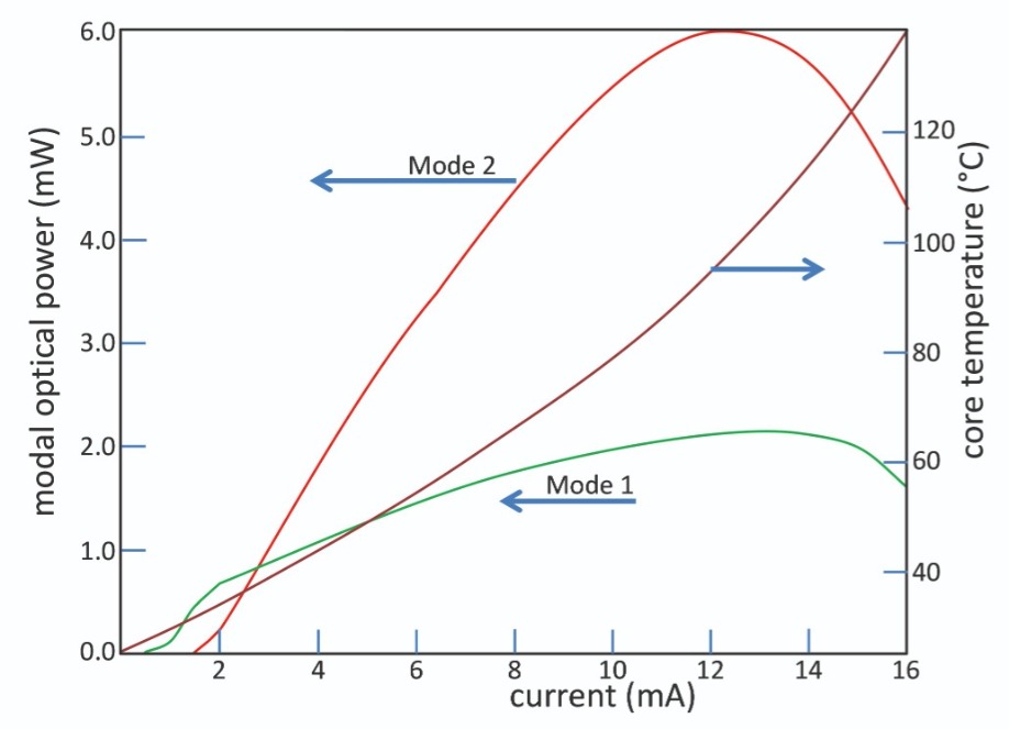
Figure 7. Light-current curves of a VCSEL, showing saturation at high currents.
Obviously, one of the goals for a VCSEL designer is to minimise heating within the device. To succeed, it is crucial to compute the heating profile and the resulting temperature distribution. Modelling with the Harold/VCSEL tool offers much insight, as shown in the plot of the temperature profile of a device driven at 16 mA (see Figure 8), using a 20 °C background temperature. In this VCSEL, there are two cavity modes. The fundamental mode starts lasing at 1 mA, but very soon a second, donut-shaped mode starts lasing. It first appears at 1.5 mA, and quickly dominates.
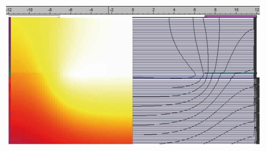
Figure 8. Temperature profile in a VCSEL, drawn as a heat-map (left) and contour plot (right).
As expected, the simulations show that as the background temperature increases, the saturation power falls. According to our calculations, the output of a VCSEL can fall by a factor of eight when the ambient temperature rises from 25 °C to 75 °C (see Figure 9). This impact poses a significant challenge for the VCSEL designer. As this is one of the most fundamental challenges in the design phase, making tools that can accurately predict the heat generation and its effect on performance is of vital importance.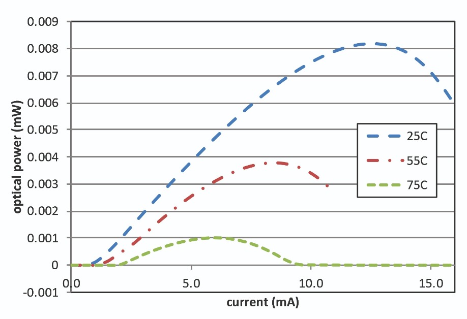
Figure 9. As the background temperature increases, VCSEL performance can drop dramatically. The graph shows the light-current curves for the same VCSEL at 25 ˚C, 55 ˚C and 75 ˚C.
A simple, obvious option for increasing the saturation power of the VCSEL is to make it bigger. Take this approach and the key lateral dimension is the diameter of the oxide window. It is this window that confines the mode laterally, rather than the walls of the VCSEL. Make this window larger, and there is a bigger surface area for heat to flow to the substrate. Alternatively, the heat flux per unit area can be maintained, allowing a proportional increase in the permitted total heat flux and ultimately the optical power.The downside of increasing the diameter of the oxide window is that it leads to multi-mode VCSEL operation. This is acceptable in many applications, so most commercial VCSELs are multi-mode. However, such devices are not really suitable for driving single-mode fibre data links – the workhorse of the datacom industry.
What may come as a surprise is that there is actually a major benefit to be had from these additional modes. Simulations show that if all the modes are artificially suppressed, save the fundamental optical mode, peak power plummets (see Figure 10). Spatial hole burning is to blame, with the low-intensity single-mode concentrated in the middle of the oxide window where the current is highest. Here the electron density builds up at the rim of the window, creating increased Auger recombination and heating. It is better to have more modes, as this ensures a more uniform optical intensity and thus a more uniform electron density.
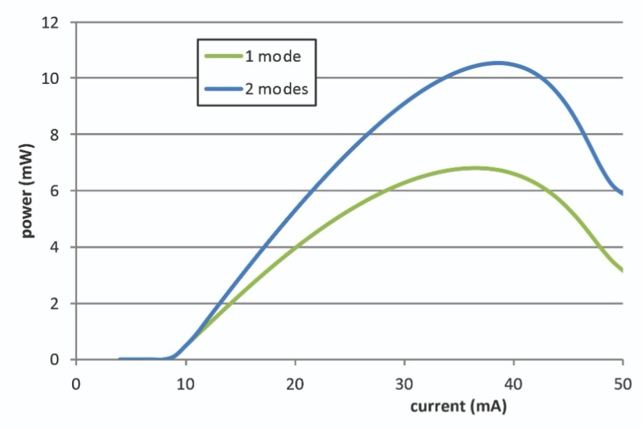
Figure 10. Light-current curves for a VCSEL, supporting two modes (blue). The second mode is suppressed (green).
Another consideration for a VCSEL designer is the gain spectrum, which has a peak that changes in amplitude and position with temperature. This can cause poor linearity in the VCSEL, exacerbated by changes in the resonance wavelength as the refractive index changes with temperature.The trick to improving linearity is judicious detuning of the mode resonance away from the gain peak. This is illustrated in Figure 11. Instead of aiming to operate the VCSEL at its room-temperature gain peak, de-tuning may be applied, leading to a far smaller reduction in gain at elevated temperatures.
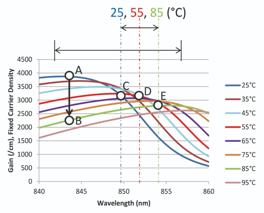
Figure 11. Computed gain spectra of a GaAs VCSEL at different temperatures. As the VCSEL heats up the gain peak moves to a longer wavelength and decreases. If the VCSEL had been designed to operate at the 25 ˚C gain peak (A), then when at 85 ˚C the gain would fall to point B. It is better to detune the VCSEL to operate at point C at room temperature, as then the gain drops by only a small amount at 85 ˚C – point E.
To try and improve VCSEL performance, several groups are exploring alternative designs. Often efforts are directed at improving the top mirror, through initiatives that include the introduction of a suspended high-contrast grating (see Figure 12). This design has many benefits: the current does not need to pass through a top DBR; light is strongly polarised; and by moving the grating with a MEMS actuator, the emission wavelength can be adjusted. Modelling of this device at Photon Design shows that realistic gratings can be designed with strong resonances, achieving a reflection of above 99 percent.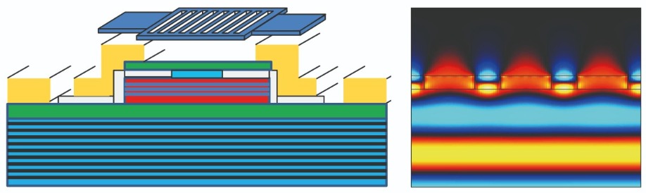
Figure 12. (left) A VCSEL that contains a suspended-grating for the top mirror. (right) the electric field generated by a plane wave incident on the grating from below – note the near absence of light above the grating.
Keeping good timeApplications for VCSELs are not limited to facial recognition and datacoms. These sources can also serve in several specialist applications, including low-power atomic sensors for precision timing. Within today’s digital infrastructure, precise clocks are critical for synchronisation. These clocks rely on signals from a global navigation satellite system for a precise timing reference. However, the satellite systems are vulnerable to incredibly costly outages, caused either accidentally or by malicious attack. If, for example, a widespread outage were to occur in the UK, it could cost the nation’s economy £1 billion per day. One solution, under development at Cardiff University and its partners, is a ‘chip-scale’ atomic clock. It could be placed within the required locations to provide a backup in the event of an outage of the global navigation satellite system.
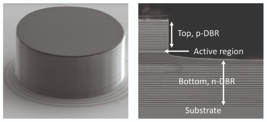
Figure 13. Side view (left) and cross-section (right) of an etched VCSEL mesa, manufactured by Cardiff University’s Institute for Compound Semiconductors.
At the heart of every all-optical atomic clock is a vapour cell, housing alkali atoms, such as caesium or rubidium. On one side of the cell is a light source, and on the other a photodetector. By clever spectroscopic interrogation, it is possible to ‘trap’ atoms in an excited state, an effect known as coherent population trapping. When this happens, the vapour cell is transparent, causing an increase in the intensity of the light that hits the photodetector (see Figure 14). As the precisely defined frequency at which this occurs is an inherent property of the atom, dialling the laser into this frequency provides a means to produce a very stable timing signal.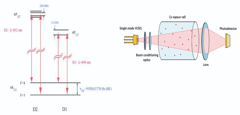
Figure 14. (left) The Caesium electron transitions used for an atomic clock targeting 894.6 nm (D1 line). (right) A caesium clock vapour cell excited by a VCSEL (courtesy of UK National Physics Laboratory).
It will not come as a surprise that the requirements for the light source in an atomic clock are much more demanding than those in most telecom applications. Requirements include: a very precise emission wavelength – for the caesium D1 line, the source must be at 894.6 nm; a linewidth below 100 MHz; a single lateral mode; and polarisation stability. In addition, because the clock must be small and portable, the light source must be compact, energy efficient, and draw less than 2 mW of power. VCSELs pose as promising candidates, particularly because their small volume quashes parasitic elements, enabling them to be modulated at the required frequency for coherent population trapping – for caesium, for example, the required frequency is 4.6 GHz. However, to fulfil all the required characteristics, much care must be taken when designing the epitaxial structure and the device geometry.To meet these specifications, a team led by researchers at Cardiff University has turned to modelling using the Harold/VCSEL tool. As well as aiding the design of the VCSEL epi-structures and device geometries, modelling assists interpretation of device results. What’s more, it offers tremendous insight into whether characteristics should be attributed to the fabrication method, or are caused by epi-growth or design.
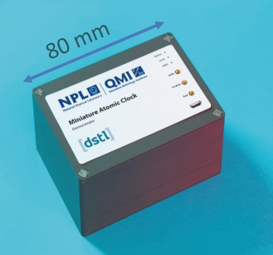
Figure 15. A packaged Caesium atomic clock with VCSEL pump (courtesy of University of Cardiff, UK National Physics Laboratory and DSTL).
There are additional benefits of modelling, specific to atomic clocks. It can help to ensure that the cavity-resonance must occur at the required wavelength, and that the active region provides optical gain with a concomitant peak wavelength, a key to efficient operation. As the vapour cell is heated, typically to 70 ˚C, these wavelengths must coincide close to this elevated temperature. That’s not easy, because the gain-peak wavelength is around four times more sensitive to temperature than the cavity-resonance.On top of all these considerations, met through careful selection of the composition and thickness of the layers in the epi-design, there are other factors that affect VCSEL performance. They depend on the way the device is fabricated.
One factor that has great influence over the performance of the VCSEL is the oxide aperture.
As atomic clocks require VCSELs to have single-mode emission, the oxide aperture is restricted to a diameter of typically no more than 3 μm. Having such a small aperture has two significant effects: it results in locally high current densities, and it alters the effective index in that region of the cavity.
The performance of the VCSEL is impaired by the high current density, which increases further with injection current. This leads to joule-heating, which can have deleterious effects not only on the optical power output, but also on the emission wavelength. Changes in power are not a major issue, as 1mW of optical power is sufficient for an atomic clock – but the wavelength is a critical parameter that needs to be precisely defined. Unfortunately, heating can shift the emission wavelength outside the intended design specification, and complicating matters even further, there can be an additional shift in emission wavelength resulting from a change in effective index, which moves the cavity resonance.
The solution is to use modelling to account for the shifts in wavelength with injected carriers and effective index variation, so that these effects can be compensated for in the design of the epilayers. Such modelling is an invaluable tool for the development and manufacture of VCSELs, which are already being produced in their billions, with volumes tipped to rise in the coming years.


