
Scientists grow optical chips in a petri dish
Miniature visible light devices use GaP waveguides embedded in perovskite light sources
A team of scientists led by researchers at ITMO in St Petersburg, Russia, have proposed a quick and affordable method to create miniature optical chips in a Petri dish. The research was published in ACS Nano.
Today's optical chips operate in the infrared (IR) range. "To make the devices even more compact, we need to work in the visible range," says Sergey Makarov, chief researcher at ITMO's Department of Physics and Engineering, "as the size of a chip depends on the wavelength of its emission."
Creating a light source that would emit in the green or red part of the spectrum is quite easy, however, waveguides for these wavelengths can be an issue.
Ivan Sinev, senior researcher at ITMO's Department of Physics and Engineering said: "The standard silicon waveguides that are used in IR optics do not work in the visible range. They transmit the signal no further than several micrometers. For an optical chip, we need to transmit along tens of micrometers with a high localisation, so that the waveguide would have a very small diameter and the light would go sufficiently far through it."
Silver waveguides were considered but the transmission distance was insufficient. In the end, they used GaP as a material for the waveguides, as it has very low losses in the visible band and long-range guiding over distances more than 20μm. But the most important thing, they say, is that both the light source can be grown directly on a waveguide in a Petri dish using solution chemistry methods, which is cheaper than the commonly used nanolithography.
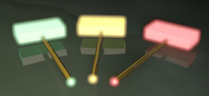
So in their chip, they embedded the GaP nanowires directly into compact CsPbBr3-based light sources. The perovskite microcrystals support stable room-temperature lasing and broadband chemical tuning of the emission wavelength in range 530–680 nm, while the GaP nanowaveguides support efficient outcoupling of light.
The size of the new chip's elements is about three times smaller than that of its counterparts that work in the IR spectral range.
"The chip's important property is its ability to tune the emission colour from green to red by using a very simple procedure: an anionic exchange between perovskite and hydrogen halides vapour," notes Anatoly Pushkarev, senior researcher at ITMO's Department of Physics and Engineering. "Importantly, you can change the emission colour after the chip's production, and this process is reversible. This could be useful for the devices that have to transmit many optical signals at different wavelengths. For example, you can create several lasers for such a device, connect them to a single waveguide, and use it for transmitting several signals of different colors at once."
The scientists also equipped the newly created chip with an optical nanoantenna made of perovskite that receives the signal travelling along the waveguide and allows uniting two chips in a single system.
"We added a nanoantenna at the other end of our waveguide," explains Pavel Trofimov, PhD student at ITMO's Department of Physics and Engineering, "so now we have a light source, a waveguide, and a nanoantenna that emits light when pumped by the microlaser's emission. We added another waveguide to it: as a result, the emission from a single laser went into two waveguides. At the same time, the nanoantenna did not just connect these elements into a single system, but also converted part of the green light into the red spectrum."
'Perovskite - Gallium Phosphide Platform for Reconfigurable Visible-Light Nanophotonic Chip' by Pavel Trofimov et al; ACS Nano, June 15, 2020


