
Verticle shrinks LEDs by chemical dicing
Using chemical dicing process, dramatic cost reduction can be achieved by substantial increase in die count per wafer
In order to improve picture quality of the mini-LED displays by increasing local dimming zones, significantly more LEDs are required than conventional LED backlight. For example, 10,000 LEDs are used to build a 12.9 inch iPad Pro screen. Consequently, lowering LED cost is the primary issue for the commercialisation of mini-LED display.
Shrinking die size would be one of the most effective ways to reduce the manufacturing cost. However, shrinking die size is limited with current die singulation technologies (e.g. the industry standard stealth laser dicing process) due to chip damage and extremely long processing time. This is particularly true for the LED die less than 100 μm.
An innovative die singulation technology, 'Chemical Dicing', enabling reduction of mini-LED die size without chip damage has been developed by Verticle. Using the chemical dicing process, dramatic cost reduction can be achieved by substantial increase in die count per wafer. Furthermore, as shown in Table1, it can result in narrower scribe street width as well.
This is attributed to a damage-free nature of the chemical dicing as it separates die by wet chemical etching the street line instead of thermal or mechanical methods which generate heat or acoustic shock waves. As a result, there are no damages around the chip edge, which means distance between active areas and chip cutting edges can be less than 2 μm. Therefore, active area can be enlarged which results in more light output from the same size LED die.

As shown in Table 1, die size shrinking and street narrowing yield dramatic DPW (die per wafer) increase up to 8X as compared with conventional flip-chip based mini-LEDs which have larger die size and wider street widths.
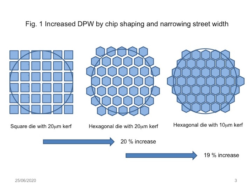
Additional DPW increase can be obtained by chip shaping. Unlike conventional die singulation methods that can only separate die in linear direction (i.e. only able to separate either square or rectangular die), chemical dicing enables free-shape die (e.g. hexagonal) formation and singulation. Hexagonal die can increase DPW by more than 20 percent due to enhanced tiling efficiency and increased usable wafer area (Fig.1).
Using this unique chemical dicing, Verticle was able to fabricate hexagonal die for the first time in the world (Fig. 2). The hexagonal shape symmetry can help better current spreading, which results in higher light output than square or rectangular die. Additionally, hexagonal die light output is enhanced after packaging as well. Hexagonal die produces a beam profile which is much closer to the circular shape of circular lens used in optics design. In contrast, the beam profile of the typical square or rectangular die, when combined with circular lens, is typically distorted.
Moreover, multiple wafers in one batch can be etched simultaneously, resulting in die singulation throughputs which are 500X greater than stealth laser dicing (Table 2).

Specialised in LED and display technology, Verticle has been established in 2004 and located in Silicon Valley, CA USA. Verticle owns the key LED patents and has more than 15 years experience in R&D and chip production.


