
Fraunhofer team reports Efficiency record for Tandem Solar Cells
Efficiency of 25.9 percent for a III-V/Si tandem solar cell grown directly on silicon marks important milestone
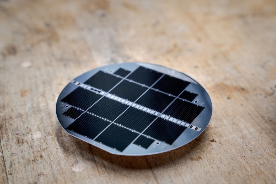
Fraunhofer ISE is now reporting a new record efficiency of 25.9 percent for a III-V/Si tandem solar cell grown directly on silicon. This cell was produced on a low-cost silicon substrate for the first time – marking an important milestone on the way to economical solutions for tandem photovoltaics.
The Fraunhofer Institute for Solar Energy Systems ISE has been working for many years on multi-junction solar cells, in which two or three sub-cells stacked on top of another absorb different portions of the solar spectrum and convert it into electricity. Silicon is a suitable absorber for the infrared part of the spectrum. Several micrometer-thin layers of III-V compound semiconductors made of elements from groups III and V of the periodic table are deposited on top of silicon. These sub-cells efficiently convert the light from the ultraviolet, visible and near-infrared parts of the spectrum into electricity.
III-V semiconductor solar cells on Germanium are often used in space as well as in concentrator photovoltaics. Through the development of better and more cost-effective processes in combination with the use of silicon as the bottom sub-cell, the tandem technology can become accessible for wide-range use in almost all photovoltaic applications in the future. However, there is still much work to be done before this objective can be achieved.
25.9 Percent for III-V/Si Tandem Solar Cells Grown Directly on Silicon
Several different approaches for producing combinations of III-V and silicon solar cells exist. For example, Fraunhofer ISE holds the world record efficiency of 34.1 (new 34.5) percent for a tandem solar cell in which the III-V semiconductor layers are transferred from a gallium arsenide to a silicon substrate and connected by wafer bonding. This technology is very efficient but also expensive.
For this reason, Fraunhofer ISE has been working for many years on more direct manufacturing processes in which the III-V layers are deposited, or grown directly onto a silicon solar cell. In this process it is crucial that all layers maintain a high crystal quality, and this presents a major challenge. Now a new world record efficiency of 25.9 percent has been achieved for a III-V/Si tandem solar cell grown directly on silicon.
The researcher Markus Feifel of Fraunhofer ISE recently presented his successful results at the 47th IEEE Photovoltaic Specialists Conference, which was held online as many conferences presently are. At this conference his work was distinguished with the Student Award in the Category of Hybrid Tandem Solar Cells. "The complex inner structure of the cell is not visible from the outside, since all of the separate absorbers are internally interconnected by additional crystal layers and electrically series connected," explains the young solar cell researcher, who was able to improve his results from 24.3 to 25.9 percent in less than a year.
"This was achieved by replacing a single thin layer within the multi-junction cell," he explains. "A careful analysis of our cells showed that this layer created a potential barrier for electrons moving through the crystal structure. “
Since 2007 the Fraunhofer researchers have been continuing to develop this technology in small steps together with the Ilmenau University of Technology, the Philipps University of Marburg and the company Aixtron, for example, setting up special epitaxial equipment and examining every single layer of the structure. These developments were funded by the German Federal Ministry of Education and Research (BMBF) as part of the III-V-Si project and the MehrSi project.
A particular highlight of the new tandem solar cell is that the III-V layers were not grown on a chemo-mechanically polished substrate as in previous cases, but directly on a silicon wafer which, after sawing was treated in a simple process using only inexpensive grinding and etching processes. The Danish company Topil developed this silicon wafer in the European SiTaSol project, thus realising an important step towards the economical production of the new multi-junction solar cells.
In the future, the focus will be to increase the efficiency even further as well as realize a faster layer deposition, with higher throughput, and thus improve the cost-effectiveness of the production. The ultimate objective is that tandem photovoltaics will be able to make an important contribution to the expansion of photovoltaics, which is necessary for the energy transition.
Key Technology for the Energy Transition
In many parts of the world today, electricity from solar cells is the cheapest form of energy generation. "In Europe the photovoltaic research community is working on numerous concepts to further improve the efficiency of this key technology which plays a central role in the energy transition," says Stefan Glunz, division director of the Photovoltaics Research at Fraunhofer ISE. "Not only are we working to make silicon solar cell production more sustainable and cost-effective, but we are also breaking new ground. We are aiming to reach even higher efficiencies using the tried and tested silicon in combination with other semiconductor materials and have achieved this in the field of tandem photovoltaics.”
This technology not only opens the door to the future of power generation but also is ideally suited for electrolysis, which is a process of using electricity to split water into hydrogen and oxygen. Thus, tandem photovoltaics can be used to produce hydrogen, an energy storage medium and important building block for the energy transition.


