
Researchers pinpoint way to improve CIGS solar cells
Reducing the density of electrically-active grain boundaries and making CIGS layers with larger grains could boost efficiency
CIGS thin-film solar cells have a maximum theoretical efficiency of about 33 percent, but the real-world efficiency has reached only around 23 percent. This shortfall is attributable to loss mechanisms in the CIGS solar cell in the functional layers and at diverse interfaces. But where exactly and why these losses occur has been a point of conjecture.
Now researchers from the Centre for Solar Energy and Hydrogen Research Baden-Württemberg (ZSW), Martin Luther University Halle-Wittenberg (MLU) and the Helmholtz-Zentrum Berlin (HZB) have identified a way to convert more sunlight into electricity in CIGS cells. They published their findings in Nature Communications in August 2020.
Reducing the density of electrically active grain boundaries boosts performance
Scientists at the ZSW, MLU and HZB have now learned more about their origins. “Some of the losses occur at the boundaries between the individual CIGS crystals in the solar cell. Positive and negative electrical charges can neutralise each other at these grain boundaries, some of which are electrically active,” says project manager Wolfram Witte from the ZSW. “This reduces the cell’s performance.”
The team were able to identify this type of loss mechanism by combining experimental measurement methods with computer simulations. The HZB analyzed a highly efficient CIGS solar cell with various electron microscopy techniques and optoelectronic measuring methods such as photoluminescence to provide realistic values to the two-dimensional device simulation developed at the MLU.
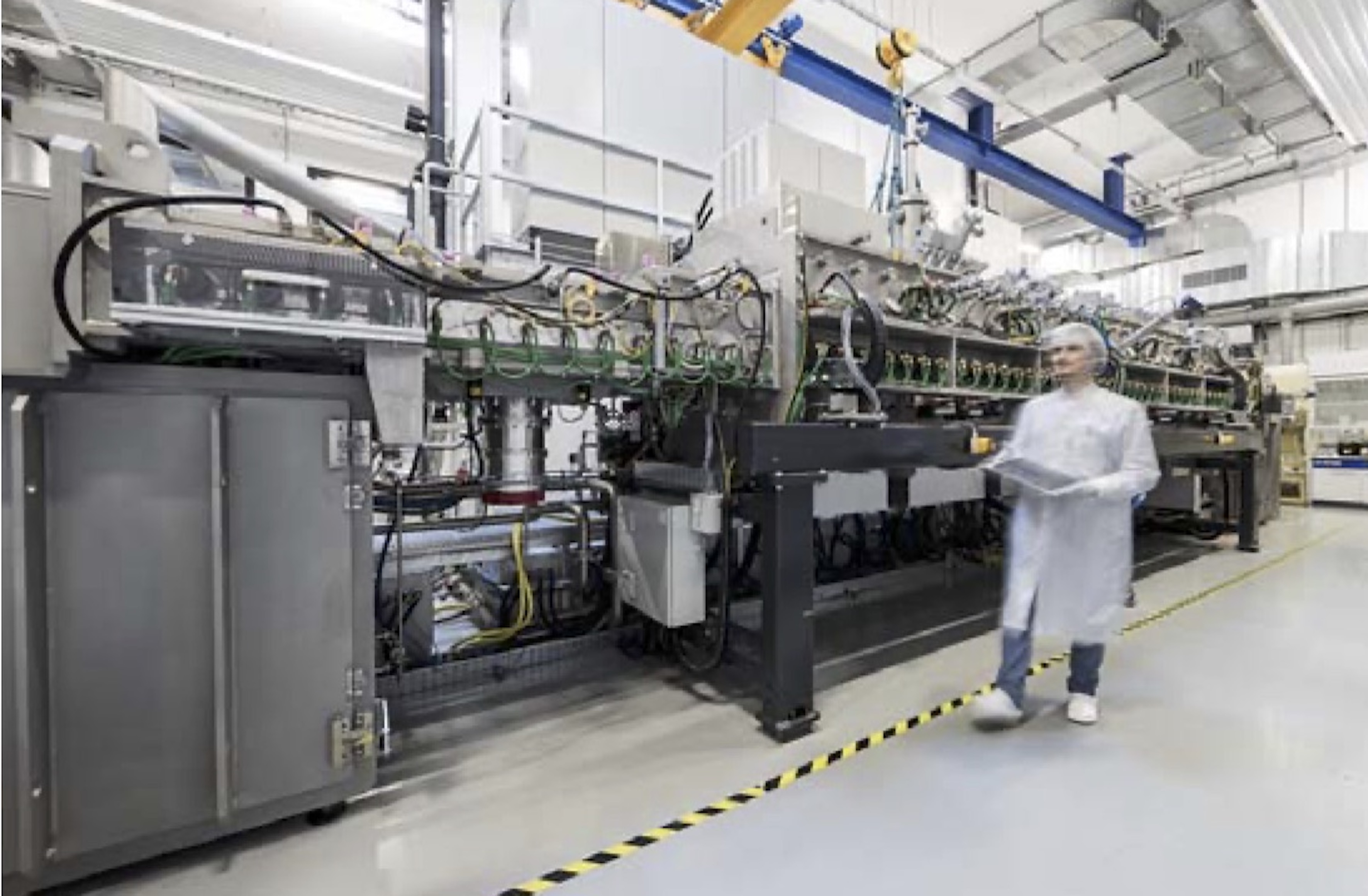
The ZSW manufactured the CIGS cell in a co-evaporation process that deposits copper, indium, gallium and selenium simultaneously in a vacuum. The cell’s efficiency was 21 percent without an additional anti-reflective layer. The physical microstructure of this cell and the values obtained in experiments with various analytical methods served as the input parameters for two-dimensional simulations.
Computer simulations showed that increased recombination at electrically active grain boundaries within the CIGS layer constitutes a significant loss mechanism. Above all, this decreases the open-circuit voltage and fill factor, which reduces the cell’s efficiency. “What needs to be done to further improve the efficiency of CIGS thin-film solar cells and modules is to reduce the density of the electrically active grain boundaries and produce CIGS layers with larger grains,” says Witte.
This could be achieved with technical means, for example, by augmenting the CIGS layer with additives, adapting the substrate material or optimising the temperature balance during coating. These would be promising points of departure for the photovoltaic industry’s efforts to elevate the efficiency of CIGS modules.
EFFCIS project
The findings described in Nature Communications were one of several partial results obtained in a joint project called EFFCIS. Funded by the BMWi, the German Federal Ministry for Economic Affairs and Energy, this research venture ended in 2020 after a run of around three and a half years. Nine partners teamed up in a consortium that had experts from research institutes, universities and industry working together under the leadership of the ZSW.
Their efforts focused on localising and learning more about the dominant loss mechanisms in CIGS thin-film solar cells and modules to then reduce or eliminate these losses with innovative measures. The partners used analytical tools with high temporal and spatial resolutions to determine the chemical and physical properties of the functional layers and interfaces in CIGS solar cells.
'Microscopic origins of performance losses in highly efficient Cu(In,Ga)Se2 thin-film solar cells' by Maximilian Krause et al; Nature Communications 11 (2020) 4189


