

Simplifying silicon-based templates
A silicon template with an incredibly thin SiC buffer layer looks set to revolutionise a range of high-performance GaN-based devices, including deep-UV LEDs and GaN HEMTs
BY Dmitry Khmyznikov, Co-founder of THE Alterphasic project AND Alexey Redkov, Senior Researcher of Alterphasic R&D team
Our industry uses silicon substrates as the foundation for manufacturing several different devices. Transphorm employs it as the bedrock for its GaN FETs, now numbering more than 500,000, and Toshiba uses it for producing GaN-on-silicon power devices. Silicon substrates also feature in microLED displays made by Plessey, and in LEDs developed by both Samsung and Bridgelux, now part of Toshiba.
There are many reasons why these chipmakers use silicon as the foundation for device production. Silicon substrates are low in cost, widely available, and allow processing in 200 mm silicon lines, which may offer very competitive production costs, while employing tools with greater levels of performance than those found in many compound semiconductor fabs.
However, producing high-quality devices using silicon is far from easy. The main issue is the significant lattice and thermal mismatch between the nitrides and the substrate. These differences induce stress and strain in the epilayers, causing wafers to bend, bow and even crack. Strain management is essential, as wafers must be flat to within several tens of microns to enable processing in silicon lines.
One way to ensure flat enough epiwafers is to introduce buffer layers that manage stresses and strains. However, this is not easy to do. Successful buffers are complex, requiring years of development. What’s more, their formation often involves depositing many layers, adding to the material costs of the epiwafer, as well as overall production costs, increased by longer growth times. Even with thicker buffer layers, dislocations are present throughout the heterostructure, hindering device performance. Yet another drawback is that the buffer may hamper thermal management, because it can increase the distance between the location of heat generation and any heat spreading technology.
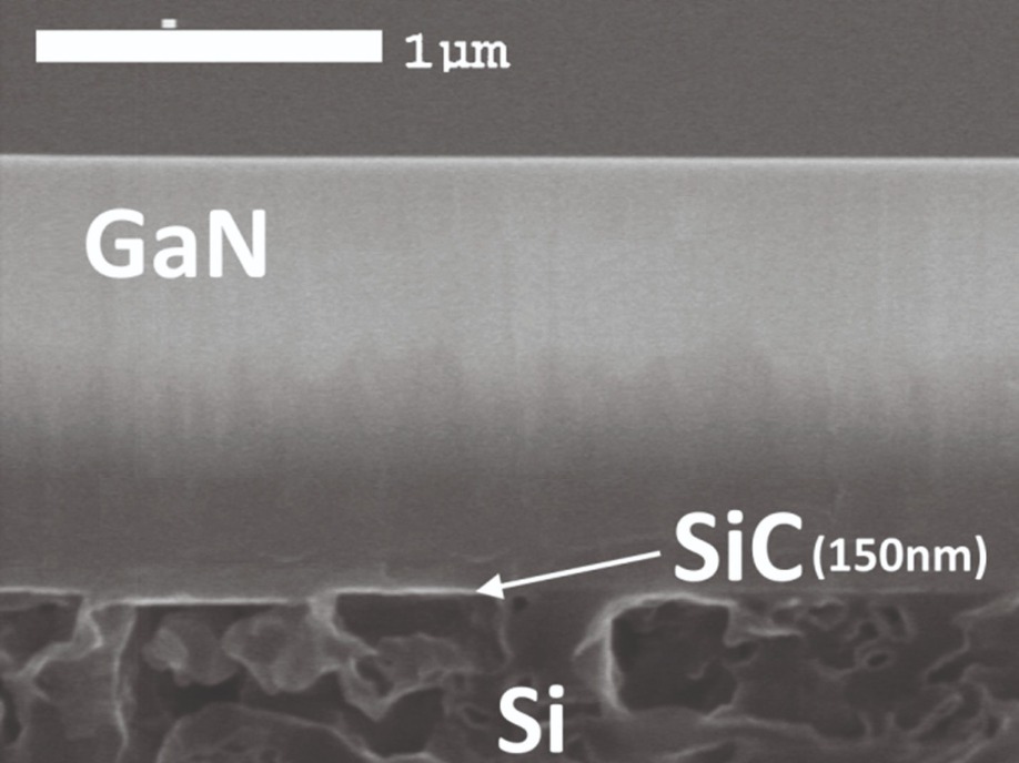
A very thin film of SiC enables the growth of high-quality GaN on a silicon substrate. The key to this success is the use of a nano-assembly method that converts a very thin layer of silicon into both cubic and hexagonal SiC.
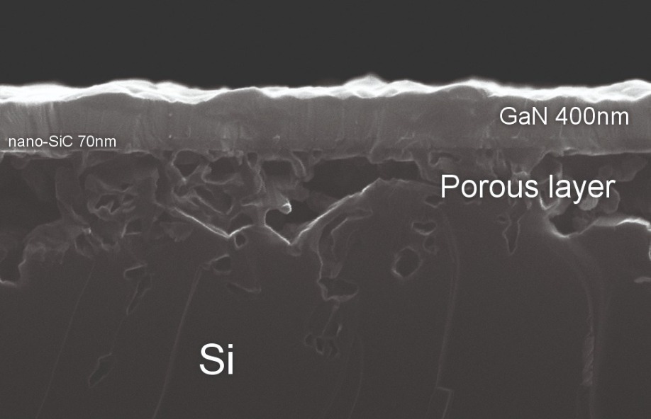
Addressing all these issues is our cost-competitive technology, developed through a project called Alterphasic, based on the fundamental work of the science team led by Professor Sergey Kukushkin, head of the laboratory at the Saint Petersburg Institute for Problems in Mechanical Engineering of the Russian Academy of Sciences. Kicked off in 2008 as independent start-up and backed by €7.5 million of private investments and grants, Alterphasic, which has led to the publication of 170 papers and 9 technology patents, has centred on the growth of an incredibly thin, monocrystalline layer of SiC on a silicon substrate. This technology yields a SiC layer of outstanding quality that provides the foundation for the growth of III-N epiwafers of various sizes. Note that it is also very easy to separate the substrate from the epilayer with our technology, due to the porous buffer layer between silicon and SiC.Turning to nano-assembly
Our technology does not involve conventional film growth, with materials deposited from above. Instead, we replace silicon atoms in a special way that retains the original crystal structure of the silicon matrix. Using this ‘nano-assembly’ method, we ‘convert’ a very thin layer of silicon into both cubic and hexagonal SiC.
During this process, we form a special porous buffer layer beneath the SiC. The top nano-SiC layer that is created provides the ideal foundation for the growth of III-Ns, thanks to the compatibility of its properties with the crystal structure of nitride heterostructures.
When epitaxial films are grown on our silicon-based templates, mechanical stress relaxation takes place. This is driven by the preliminary embedding of the substrate lattice through assembly of nano-objects. By ensuring that carbon atoms are positioned at interstitial positions of silicon and silicon vacancies, we create a so-called ‘dilatation dipole’.
Unlike traditional epilayer growth, the orientation of our films is determined by the crystal structure of the original silicon matrix, rather than just the substrate surface. We have found that the best way to produce a cubic crystal is to form a dilatation dipole that is perpendicular to the (111) plane of silicon. When this occurs, almost all the elastic dilation energy of the film relaxes due to dipoles alone, leading to high-quality SiC films.
A high-quality epitaxial layer of GaN is gown by HVPE on a hybrid nano-SiC-on-silicon substrate.
A great strength of our hybrid nano-SiC-on-silicon substrate is its simplicity, allowing it to be easily incorporated into the manufacturing process of many fabs. Using our materials technology, engineers can manage complex growth processes, starting with a surface containing very few defects. To demonstrate our technology, we have produced uniform films across the whole surface of p- and n-type silicon wafers with diameters of 1-inch, 2-inch, 3-inch, 4-inch, and 6-inch. That’s not the upper limit for our templates – it is determined only by the size of the reactor chamber and the diameter of the silicon substrates that are available.To demonstrate the promise of our technology, we have used it to produce a wide range of thick, single-crystal, low-defect layers of various III-Ns using HVPE. This includes conventional GaN, AlN, AlGaN, and also a variety of semi-polar forms of GaN. Examples of nano SiC-on-silicon substrates that we have made, reproduced and tested in the lab include: AlN layers with an orientation (0001) and thicknesses ranging from just 40 nm to 700 μm, using silicon orientations (111) and (011); and semi-polar epitaxial AlN layers with the orientations (1120), (1013) and (2023), using silicon orientations (001) and (310).
Additional results include the growth of AlGaN layers with a (0001) orientation that have thicknesses between 100 nm and 400 μm, formed using SiC-on-silicon (001) substrates. We also separated layers with a thickness of 400 μm from the template.
Using our technology, we have produced a portfolio of monocrystal layers that are completely free of cracks. As well as AlGaN layers with a thickness up to 400 μm that we have just mentioned, we have made AlN with a thickness up to 300 μm, GaN with a thickness up to 200 μm and semi-polar (1124) GaN.
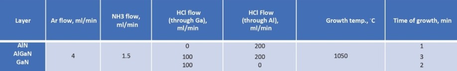
We have determined the growth rates for a variety of III-N films grown on our SiC-on-silicon templates, using the growth conditions detailed in Table 1, and layer thicknesses determined by electron microscopy. Films of GaN, AlGaN and AlN had thicknesses of 2.2 μm, 1.82 μm and 0.72 μm, respectively, while the SiC layer is just 70 nm-thick. This implies a growth rate for a GaN layer of 66 μm/hr, that for an AlGaN layer of 36 μm/hr and that for AlN of 42 μm/hr. The growth process still can be further optimized for higher growth rates.
A range of high-quality, thick films of III-Ns can be grown on Alterphasic’s nano-SiC-on-silicon substrates using HVPE.
To inspect the degree of strain in these III-N films grown on our templates, we have turned to Raman spectroscopy. This powerful technique confirms the composition of the films and reveals that layers grown on the SiC-on-silicon substrate are only very lightly elastically stressed. Based on these findings, and the growth rates, it is clear that our novel templates can be used to grow high-quality, thick layers – that is, up to tens of microns – at very high growth rates.Simple substrate separation
For some devices, such as UV LEDs, it can be useful to remove the silicon substrate, as this can absorb light and hold back efficiency. Thanks to the porous layer between silicon and the incredibly thin layer of SiC, we can employ a very simple chemical etching process, taking a matter of minutes, to separate the thin films or heterostructures from the silicon substrate. The freed material can provide a foundation for further bulk crystal growth, or be attached to another substrate.
Many devices could benefit from the high-quality, III-N layers formed with our silicon template technology. Our breakthrough could aid the manufacture of III-N transistors, as well as visible and UV laser diodes, LEDs and VCSELs. When these optoelectronic devices are grown on the conventional planes of III-Ns, efficient radiative recombination is hampered by strong internal electric fields. Switching to the semi-polar planes we have produced alleviates this, unlocking the door to more powerful light emitters.
To demonstrate the capability of our technology at the device level, we are using our SiC-on-silicon templates as a foundation for HEMTs and deep UV LEDs. For the latter, we start with a layer of AlGaN. We see this as a better choice than AlN, a material that seems incompatible with reasonable levels of p-type doping. Even in layers of AlGaN, realising p-type doping is a challenge, due to the high ionization energy of acceptor impurities. Efforts on this front are also hampered by the strong interaction of acceptor impurities with various structural AlGaN defects, leading to the formation of deep levels associated with both acceptors and donors. This work is still in its infancy, with successes to date including the fabrication of AlGaN layers with an aluminium content close to 50 percent.
Such efforts are showcasing the capability of our novel templates, and their capability to transform the production of various wide bandgap electronic and optoelectronic devices that benefit from increased material quality. Costs of chip production should also plummet with our templates, due to a drastic reduction in the cost of growth of these structures, a significant simplification of the growth technology, and the scalability on offer by turning to substrates with large diameters.

Further reading
S.A. Kukushkin et al. J. Phys. D: Appl. Phys 47 313001 (2014)
S.A. Kukushkin et al. J. Appl. Phys. 113 024909 (2013)
www.alterphasic.com


