
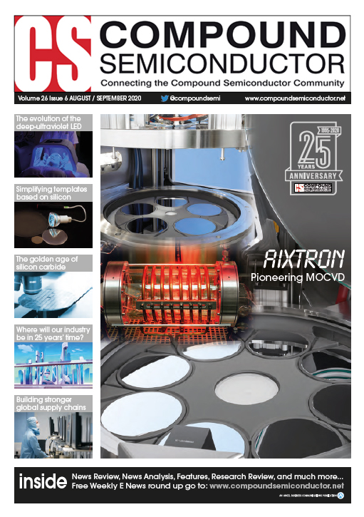
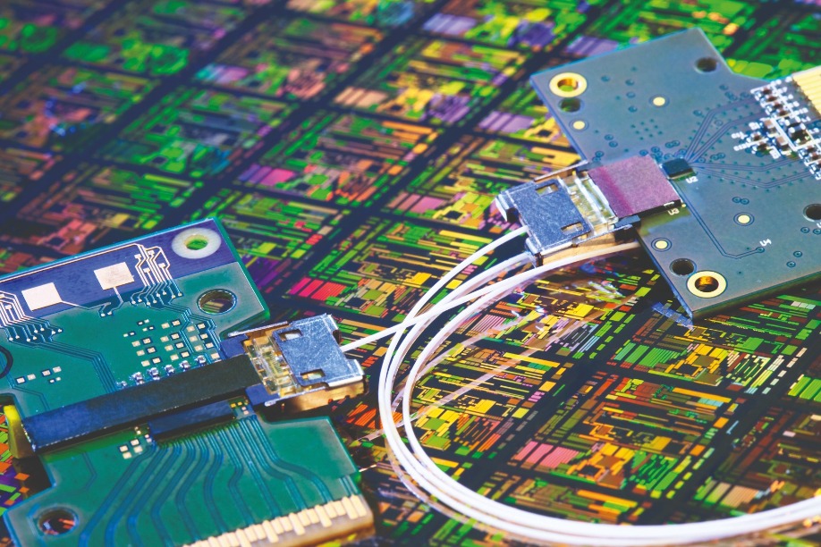
Retrospective: 1995-2020
It is staggering how much we have accomplished over the last 25 years. We have invented several devices and manufactured a variety of widely deployed, highly valued chip technologies. Our triumphs include: the development of blue and green GaN lasers, variants that emit from the surface of these chips, and a portfolio of gallium oxide power devices; the high-volume production of powerful LEDs that backlight screens and have revolutionised the light bulb; the commercialisation of SiC diodes and transistors that are driving increases in the efficiency of electrical circuits; and the construction of GaAs fabs that have churned out billions of amplifiers, a key ingredient in mobile phones. Read on to hear about all these successes and many more, as we take a look at the biggest story for every year, starting way back in 1995, when this magazine made its debut.
1995: A brilliant laser
By summer 1995, Shuji Nakamura, trailblazer of efficient blue LEDs, had already become an industry celebrity. After inventing this device in 1993, he remained in the limelight by setting a series of ever higher benchmarks for the performance of this light-emitting chip. These successes enriched his standing within the tech pantheon of all-time greats and brought many accolades, including the biggest of all, a Nobel Prize for Physics, coming in 2014. But he got even greater pleasure from seeing his work laying a foundation for a lighting revolution.
While Nakamura is undoubtedly renowned for contributions to the development of the GaN LED, it is by no means the only ubiquitous device he has invented. He is also the originator of the cousin of the GaN LED, the GaN laser diode. The latter is an astonishing triumph. While many manufacturers are making millions of GaN LEDs every month, 25 years on from its introduction, there are still only two high-volume makers of the GaN laser diode: Nichia, where Nakamura worked throughout the 1990s; and Osram Opto Semiconductors of Regensburg, Germany.
Nakamura’s laser breakthrough came in late 1995, with news breaking on 12 December. Nichia’s greatest engineer appeared on TV later that month on a national evening news broadcast, demonstrating his wonderful new device.
By early 1996, details of the laser diode started to appear in the scientific press. A paper in the Japanese Journal of Applied Physics described a 30 μm-wide, 1500 μm-long stripe laser grown on a sapphire substrate. Emitting at 417 nm, it had an active region containing 26 quantum wells, each made from a 2.5 nm-thick layer of In0.2Ga0.8N. To get this device to lase, the voltage had to be cranked up to 34 V. Driven in pulsed mode at even higher voltages, this chip produced an output of more than 200 mW. Encouragingly, this laser showed no signs of degradation after two hours of operation.
Even before its debut, the entire optoelectronic industry had little doubt regarding the killer application for this short-wavelength laser diode. Back then most music lovers bought CDs, VHS recorders were on the verge of being replaced by DVD players, and even better picture quality was now on the horizon, thanks to a five-fold hike in storage density enabled by blue-violet lasers.
Those keen to splash out on a new generation of disc players that would allow them to watch high-definition movies in their own homes had a really tough time. Early adopters began by getting caught up in a format war between the advocates of HD DVD technology and those giving their backing to Blu-ray. When that had been resolved, allowing customers to pay top whack for one of the first Blu-ray players that hit the shelves in Japan in 2003, further frustration followed – those early adopters had to wait several years for the launch of the first titles.
Fortunately, some good years followed, providing a growing, lucrative market for the blue laser diode. Since then the increasing uptake of streaming services has sent sales of Blu-ray players into terminal decline – but as this door has shut, several others have opened. Blue lasers are now being deployed alongside red and green variants in colour projectors, and they are used also in copper welding systems, where they operate at an absorption sweet spot, enabling excellent welds. There is also the possibility that one day lasers will replace LEDs in general lighting – so maybe, just maybe, there will come a time when society is as thankful to Nakamura for his laser as they are for his LED.
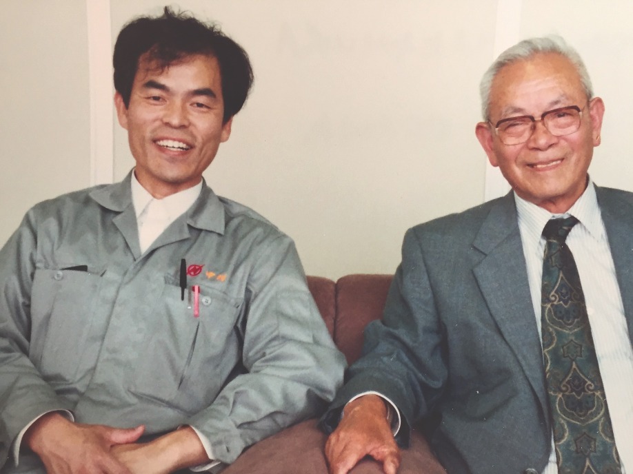
Shuji Nakamura, inventor of efficient GaN LEDs and GaN lasers, sitting next to Nobuo Ogawa, founder of Nichia. Credit: Bob Johnstone.
1996: Photovoltaics fly high
Back in 1985 very few owned a mobile phone. Those that did included Karen Bertinger, the wife of a Motorola executive, who tried to reach her husband while holidaying in the Caribbean. Her call failed to get through, convincing the intended recipient, Barry Bertinger, of the need for a truly global wireless communication network. To build this, Motorola founded and financed Iridium, a spin out that would advance telephony through the launch of 66 satellites, all placed in low-earth orbits.
By 1996 makers of III-V photovoltaics were busy producing the devices for powering these satellites. Although silicon cells were still winning sales in the space sector, single-junction GaAs devices were in the ascendency. Despite costing five-to-eight times as much as their silicon siblings, they were favoured due to their higher efficiency. At the start of their life, they had an efficiency 25 percent higher – and crucially, at the end of life, after being battered by radiation, they were 40 to 60 percent more efficient. Given that each Iridium satellite required 24 m2 of GaAs cells, using these devices rather than those made from silicon led to a significant reduction in the solar-cell footprint.
Helping to fulfil orders for GaAs solar cells were a pair of Californian photovoltaic manufacturers: Spectrolab, at the time a subsidiary of Hughes and now part of Boeing; and Tecstar. For the latter, thanks to involvement in the Iridium project, production in 1996 totalled 200,000 3-inch wafers, equating to 140 kW of power.
Engineers produced these cells on germanium substrates. They were half the price of those made from GaAs, and much stronger. This use of germanium generated much business for the makers of the raw material – the price of high-purity polycrystalline germanium rocketed, climbing by a factor of seven in just 18 months – and ramped sales for two leading substrate makers, the US firm Eagle Pitcher and the Belgium outfit Union Minière, now known as Umicore. In 1996 germanium substrate consumption totalled between 300,000 and 500,000, with sizes ranging from 1.5 inch to 4 inch.
On 1 November, 1998, the Iridium network launched to much fanfare, with the first call placed between US Vice President Al Gore and Gilbert Grosvenor, great-grandson of Alexander Graham Bell.
However, despite this great publicity, the service never caught on. Potential customers balked at paying $2500 for the handset. Dropping this to $1495 and slashing service costs to two-thirds failed to turn the business around, and even by the end of 1999 Iridium had just 15,000 subscribers, a far cry from an anticipated 500,000. An inevitable filing for bankruptcy followed.
Failure of the venture took its toll on photovoltaic maker Tecstar. In 2001 it tried to branch out into LED epiwafers. Diversification did not go well, and in 2002 Tecstar’s management decided to call it a day, selling it solar division to Emcore for $21 million. Today, the technology is in the hands of SolAero, formed in late 2014 through the sale of Emcore’s solar power business.
With 66 satellites each requiring 24 m2 of GaAs solar cells, the Iridium project, which aimed to provide global cellular coverage, generated much revenue for the III-V photovoltaics industry. Credit: Eric Long, National Air and Space Museum, Smithsonian Institution.
1997: Growth for gallium arsenide
Owning a mobile may not have been the norm in the early 1990s, but it became increasingly common towards the turn of the millennium. The uptake of these handsets helped to swell the sales of makers of GaAs microelectronics, and provided the impetus for several of these firms to reach milestones, including three in 1997: the launch of RFMD on the stock market, the shipment of Rockwell’s two-millionth HBT, and Anadigics’ sale of its millionth GaAs IC.
RFMD, now part of Qorvo, started out as a fabless supplier of GaAs MESFETs, silicon bipolar devices, and HBTs, which provided 85 percent of sales. As demand for the latter ramped, RFMD couldn’t keep pace, losing a key contract with Qualcomm.
To prevent this from happening again, RFMD built its 4-inch GaAs fab in Greesnsboro, NC, in the late 1990s. Constructed in two phases, the facility initially produced 10,000 wafers per year, before eventually increasing to 25,000. Funding for this facility came from an IPO, supported by RFMD’s source of HBT wafers, TRW. It would become RFMD’s biggest shareholder, taking a 31.1 percent stake in the company.
For Rockwell Semiconductor Systems, the latter half of the 1990s will be remembered for an explosive ramp in the production of its HBTs, made in its 4-inch fab. During the 18 months spanning the beginning of 1996 to the middle of 1997, production at this company – which went on to form Skyworks Solutions in 2002 through a merger with Alpha Industries – mushroomed from just 10,000 units per month to 70 times that figure. Buyers of these HBTs included Qualcomm and Samsung. Both valued this class of transistor for its combination of excellent linearity and high efficiency, attributes ideal for making handsets based on CDMA technology that featured long talk times.
Rockwell faced competition for this business from Anadigics, which had shipped more than a million GaAs ICs supporting the CDMA standard by summer 1997. While most of Rockwell’s HBTs were being incorporated into phones operating in the 800 MHz to 900 MHz band, parts for Anadigics were providing amplification in transmitters of handsets using spectrum at 1900 MHz.
These higher-frequency products, based on Anadigics core technology, the MESFET, initially positioned the company for future success – but further ahead, contributed to its decline.
By the late 1990s, handset makers had shifted from using 6 V batteries to those providing 4.5 V and then just 3 V. This played into the hands of the increasingly price-competitive HBT. By the early 2000s, Anadigics ceased production of its MESFET, fighting back by developing a new generation of HBT.
Instead of having an AlGaAs emitter, it used InGaP. This refinement increased the HBT’s reliability, bolstered its high-temperature operation and improved its linearity. Anadigics’ product eventually proved a hit with handset makers, giving the company a healthy share of the 3G market.
1998: A fabulous fab
When you think of high-volume manufacture of GaAs microelectronic devices, you’ll probably think of HBTs for smartphones. But that’s not the only market that has existed. In the telecommunications sector, a great deal of GaAs has been produced for laser and modulator drivers, multiplexers, demultiplexers, transimpedance amplifiers, clocks, and data-recovery circuits. In all these components, the higher speeds wrought by GaAs over silicon CMOS have yielded higher bit rates.
Back in 1998, when GaAs devices for the telecoms sector were flying off the shelves, Vitesse increased the production of products by building the world’s first 6-inch GaAs fab.
Unlike most construction projects, where deadlines come and go, Vitesse’s facility in Colorado Springs, CO, came in more than three months ahead of schedule. The first products, featuring GaAs MESFET technology, came off the line in early 1998, and in the third quarter of the year the company shipped $15 million of chips, based on 16 different products.
Vitesse, which also led the world in the migration from 3-inch to 4-inch GaAs production, built the 6-inch fab to cut the cost per die. Despite incurring a 25 percent hike in substrate-cost-per-unit-area, the switch to larger wafers delivered a 40 percent reduction at the die level.In the markets that Vitesse served, its technology had to continue to advance so that it could maintain a safe distance from products based on silicon CMOS.
The bursting of the dot.com bubble dealt a cruel blow, causing sales for Vitesse’s 40 Gbit/s devices to collapse and not recover before a 90 nm silicon process had caught up. This ultimately led to the closure of Vitesse’s GaAs fab in 2003.
After that, the company shifted focus, concentrating on silicon-based products for the metro, enterprise and storage market; and used its 4-inch InP fab to make high-speed electronic devices. The final chapter in the company’s history came in 2015, with its acquisition by Microsemi.
Even today, a 6-inch fab represents the state-of-the art for producing GaAs transistors. This might suggest that in the last two decades progress in chip manufacture has stalled. But consider this: in silicon CMOS fabs, the rapid advances in wafer sizes through the last three decades of the twentieth century have not continued into this millennium, and there may never be a 450 mm silicon fab.
For silicon, the 300 mm fab appears to be the sweet spot for production, with the investment required for any larger size failing to offer a suitable return – and for GaAs, the same could apply to the 6-inch line.
1999: The perfect marriage
What makes for an ideal merger? In a nutshell, it occurs when the result is greater than the sum of its parts.
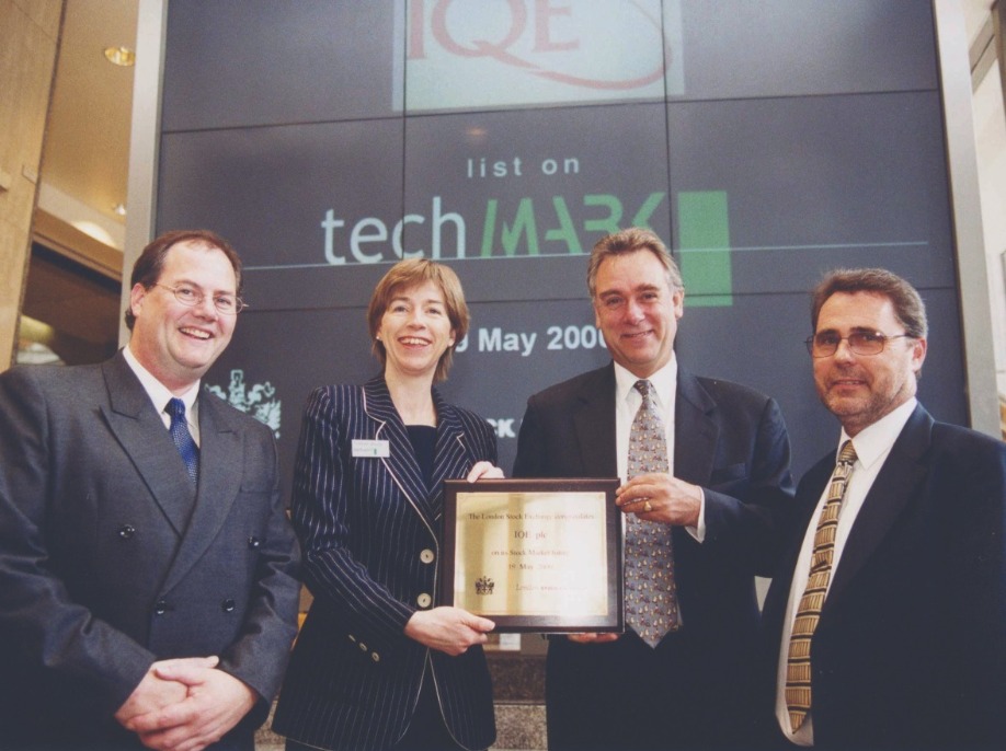
That appears to have taken place when Epitaxial Products International (EPI) joined forces with Quantum Epitaxial Design (QED) in 1999 to create IQE, the world’s largest epiwafer supplier. EPI of Bethlehem, PA, had built up its business by supplying MBE-grown wafers, used to make electronic devices, to a predominantly domestic market; while UK-based IQE had focused on optoelectronic epiwafers, with two-thirds of its sales coming from Europe and Asia.
The merged entity, offering a dual source of supply for some products, promised to be a resounding global success, drawing on the growing businesses of both companies. Sales at QED were increasing at a compound annual growth rate of 40 percent, while at IQE they were ramping at 30 percent. To cater for greater demand both sites had capacity expansion plans in place. QED had an order in for an MBE reactor capable of producing multiple 6-inch wafers from a single run, and EPI, which had recently increased the size of its facility, had placed orders for multi-wafer MOCVD tools. Helping to fund these expansion plans, IQE raised $70 million in an IPO, launching on the EASDAQ, the European version of NASDAQ, in summer 1999.
Since then IQE has strengthened its leading position in the epiwafer market. In 2006 it acquired the epi business of Emcore; the following year it bought MBE Technologies of Singapore; and in 2012 it acquired the epi-business of RFMD. It has also broadened its portfolio. The company added technology for realising high-quality GaN in 2009, by buying NanoGaN of Bath, UK; the purchase Galaxy Semiconductor of Spokane, WA, in 2010, equipped the multi-national with capability in antimony substrates and infrared technology; in 2012, the investment in Solar Junction strengthened expertise in multi-junction solar cells; and in 2018, the acquisition of Translucent’s technology brought on board capability in crystalline rare-earth oxides, enabling compound semiconductor films to be grown on silicon wafers. IQE is now a colossus in epiwafer manufacture and related technologies.
In 1999 the merger of UK-based Epitaxial Products International and US-based Quantum Epitaxial Design spawned IQE, which launched on the European equivalent of the NASDAQ.
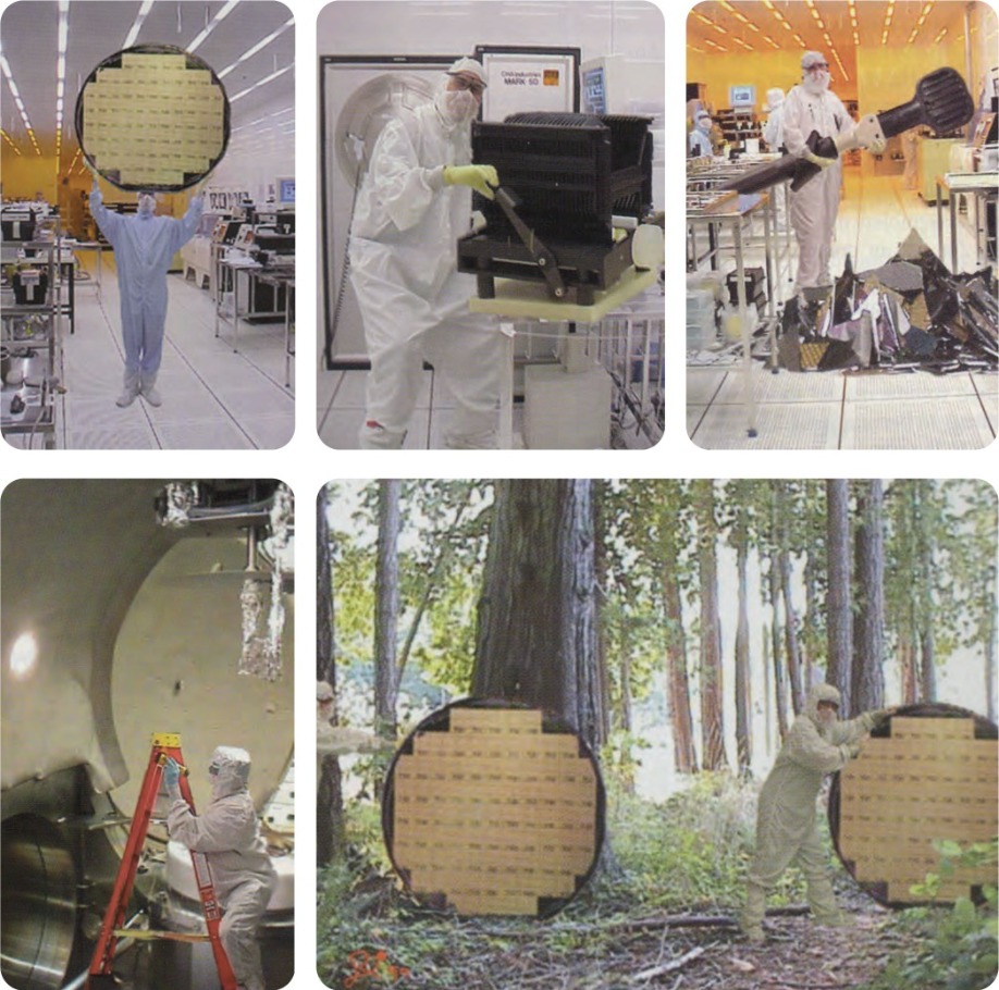
In the late 1990s and early 2000s GaAs fabs were transitioning to larger wafers. Injecting some humour into the race to gain bragging rights with ever larger lines, TriQuint provided ‘evidence’ of its 6-foot fab in a series of images, described in chronological order. (top left) TriQuint announced the start-up of the industry’s first 72-inch wafer assembly line by circulating a press release at the GaAs Mantech conference held in 1999. (top middle). TriQuint then revealed that some of its engineers had been working frantically to prevent heavy lifting. “Man these are some big GaAs-wafers,” commented one operator (top centre). In the next picture story (top right), a TriQuint technician remarked: “I don’t know what happened, it just fell off the wand!” TriQuint went on to explain how equipment maintenance can prove to be quite a chore in a 72-inch wafer fab. This equipment engineer is inspecting just one of the many massive vacuum chambers used in the evaporation process. (bottom left) In the final release (bottom right), TriQuint reported how excitement built at the 72-inch wafer plant as the first finished wafers were distributed through the ‘Silicon Forest’.
2000: Giddy highs
Internet traffic soared in the run up to the millennium, placing tremendous strain on optical communication infrastructure. Carriers addressed this by beefing up network capacity. This created an optical component sector worth almost $10 billion and tipped to increase at a compound annual growth rate of 40 percent. Makers of III-V optoelectronics were well-positioned to benefit from this ramp, as their devices accounted for up to half that market.
Understandably, frantic carriers did not want to deal with numerous component suppliers. They longed for one-stop shops, ideally offering modules that would drop into their networks.
To cater for this demand, acquisitions ran rife in the components sector. JDS Uniphase (JDSU), formed in June 1999 through the merger of the Canadian outfit JDS Optics and the US firm Uniphase, led this spending spree. In late 1999 JDSU signed a deal worth $400 million for photodetector maker Epitaxx, and in 2000 it made three monumental acquisitions: it snapped up Optical Coating Laboratory for $6.2 billion, E-Tek Dynamics for $15 billion and SDL Lasers for a whopping $41 billion.
Once the dot.com bubble had started to burst in the first few months in the new millennium, everyone knew the folly of buying a company for figure that is many times more than its annual revenue. That made the purchase of SDL, for which JDSU had forked out a sum equating to 142 times the annual revenue, an outrageous blunder. Hindsight exposed any notion of a new world order, rampant in the giddy highs, and traditional economics were back with a vengeance.
During 2000, inventory corrections kicked in within the supply chain, driving down margins. On 30 June of that year JDSU had the dubious distinction of reporting the biggest ever annual corporate loss – an eye-watering $ 56.1 billion (taking inflation into account, it’s now in fourth place, behind AOL Time Warner, American International Group and Fannie Mae). However, for JDSU this loss was predominantly on paper. The vast majority of the $56.1 billion came from a write down of goodwill associated with various acquisitions, which were primarily all-stock deals.
For investors, the downturn in company fortunes could not be dismissed so easily. In March 2000, spurred on by analyst claims that out-of-the-box visionaries were leading a great company in exactly the right place at the right time, shares in this Wall Street ‘darling’ peak at $1200. Go forward a few years and they had fallen by more than 99 percent.
The company’s leaders sold some of their shares near their peak, leading to accusations of fraud and insider trading. Some joked that JDSU now stood for Just Don’t Sue Us – and those representing the state of Connecticut did just that, hoping to recover losses from a pension fund. The case, filed in 2002, came to court five years on, with management cleared of fraud.
By then the company CEO of the glory days, Kevin Kalkhoven, had retired, using part of his wealth for philanthropic ventures. He also funded a car-racing team that notched up five victories, including the Indianapolis 500 in 2013.
As for JDSU, it no longer exists. The prolonged downturn in the optical component business took a heavy toll, with the company shedding 80 percent of its workforce and closing 29 sites. In August 2015 the company split, forming network test and measurement specialist, Viavi Solutions and the laser manufacturer Lumentum.

Kevin Kalkhoven, former JDSU CEO, co-founded PKV Racing, later known as KV Racing Technology. This team competed in both the Champ Car World Series and the IndyCar series, amassing five wins, including the 2013 Indianapolis 500.
2001: A powerful start
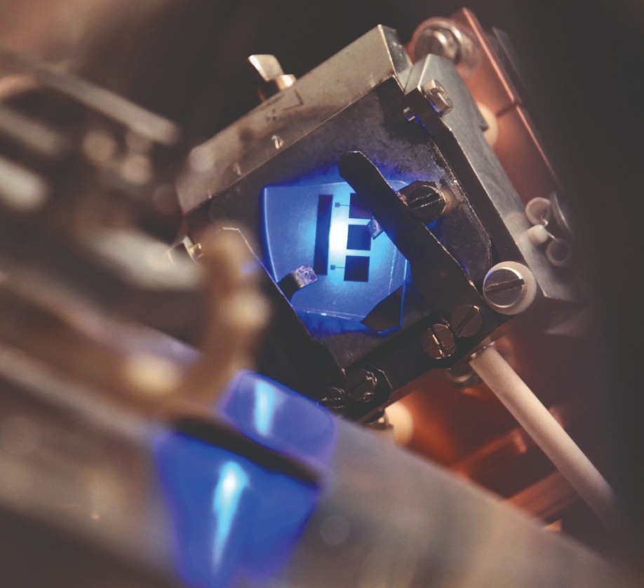
What marked the beginning of the wide bandgap power electronic industry? It is surely Infineon’s launch of the SiC Schottky barrier diode, the first wide bandgap power electronic product to hit the market.
When this device made its debut in 2001 it filled a gap in the market. Silicon and GaAs Schottky barrier diodes were limited to blocking below 250 V to avoid very high leakage currents, exacerbated at high temperatures. Infineon’s pair of variants could handle 300 V and 600 V while carrying up to 1 A, and were far better at handling heat, giving them an edge for deployment in power supplies.
Infineon, which made these devices from 2-inch SiC wafers at its fab in Villach, Austria, targeted power supplies operating between 200 W and 1000 W. Used in that manner, the company’s diodes featured in servers and wireless base stations.
The designers willing to make the switch from silicon diodes to those made from SiC were well rewarded. Their supplies were more reliable and more efficient, and they could be smaller and lighter, as the SiC diodes allowed the operating frequency to increase, opening the door to a reduction in the size and weight of passive components.
Infineon’s first generation of SiC diodes sported a simple architecture, selected to try and minimise costs that were dominated by pricey 2-inch SiC substrates.
Since then substrates have increased in size and quality and fallen in price and diodes have been through several iterations, increasing in complexity. By 2018, Infineon had reached its sixth generation, a family of 650 V SiC Schottky barrier diodes capable of handling currents ranging from 4 A to 20 A.
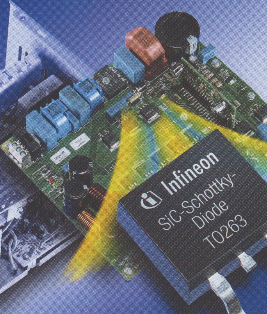
The birth of the wide bandgap industry came in 2001, with Infineon’s launch of the SiC Schottky barrier diode.
2002: Hooray for handsets
The compound semiconductor industry can never be accused of putting all of its eggs in one basket. But at the start of this century, it certainly placed two of its largest in there. Back then handsets provided the killer applications for: LEDs, used to backlight screens, illuminate keypads and provide camera flash; and GaAs transistors, used to amplify and switch
RF signals.
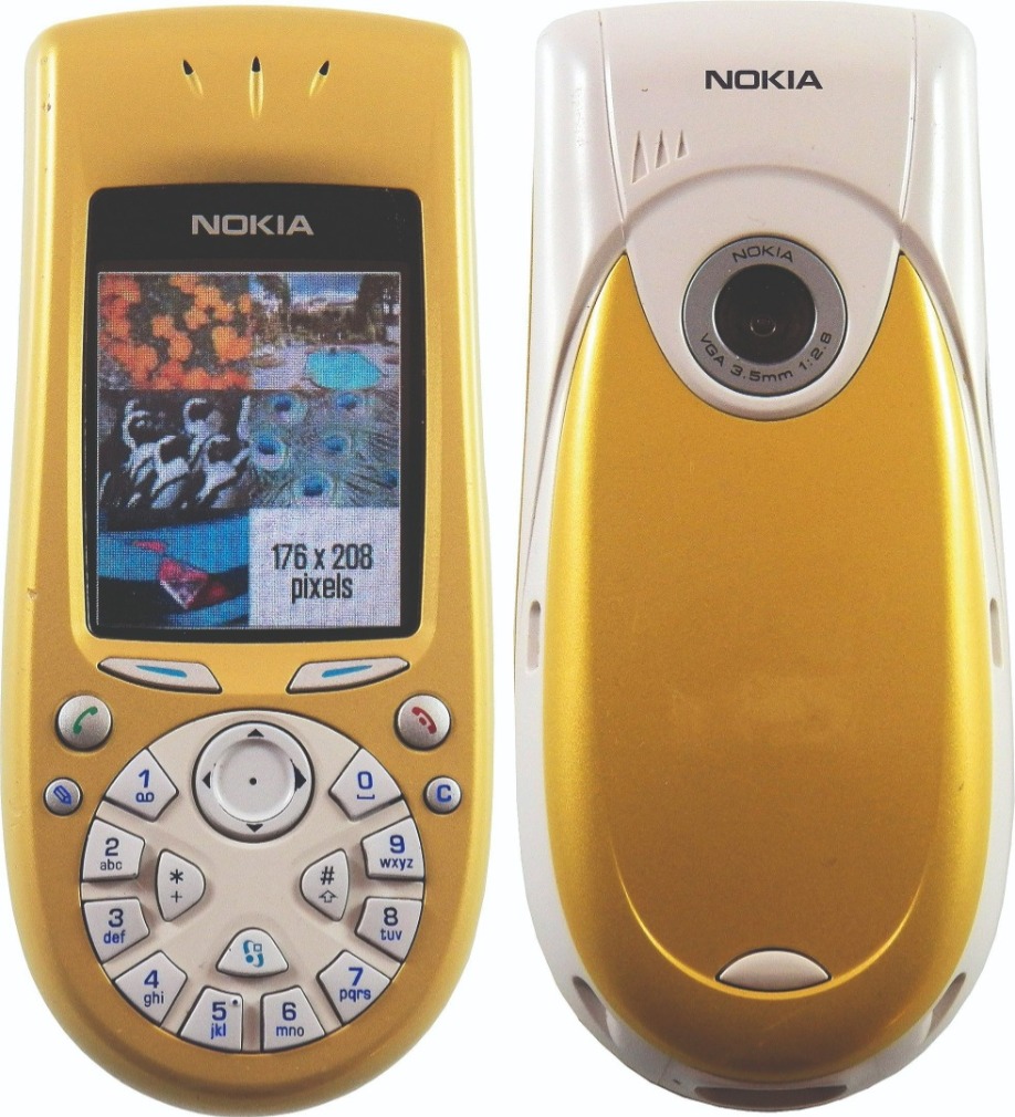
When the mobile phone industry was in its infancy, the focus would have been on attracting new customers. But within a few years efforts had broadened to include attempts to woo owners to upgrade their devices. In 2002, the cool new features were colour screens, built-in cameras, and picture and photo-messaging services.
In Japan, mobile network operator J-phone offered those that purchased a new handset the opportunity to send five second video clips accompanied by sound. Over the last two decades, the leading brands have changed markedly, shifting the fortunes of the makers of GaAs microelectronics.
In early 2002, when phones supporting 2.5G led the way, Nokia dominated the market with a share of more than 35 percent, providing GaAs-HBT manufacturer RFMD with about half its shipments.
Motorola occupied second spot with 16 percent of the market, followed by Samsung, Siemens, and Sony Ericsson. Fast forward to 2019 and Samsung had moved up to pole position, followed by Huawei, Apple, Xiamoi and then Oppo.
There has also been a substantial rise in annual phone sales. In 2002, this totalled just over 400 million, while last year almost a billion more were bought. A forecast made earlier this year suggests sales will fall by 200 million this year, due to the financial impact created by Covid-19.
The introduction of colour screens in handsets in the early years of this millennium helped swell sales of LEDs.
2003: Tumultuous times for telecos
As we emerge from the pandemic, many are wondering what shape the economic recovery will take. We hanker for a “V” – that is, that after the sharp decline there will be an equally sharp rise that speeds us to a time of steady, sustained growth. Unfortunately, probably the best we can hope for will be a “U”, with a few tough quarters in store before we return to better days. What we are desperate to avoid is an “L”, a decline that leaves a permanent scar on the economy.
Sometimes some sectors will experience an “L”, even when the general economy is on the up. That happened to component makers within the telecommunications market in the ‘noughties’,
leading to a flurry of activity in 2003. When the dot.com bubble started to burst, the III-V chipmakers operating in this industry initially put the problem down to inventory corrections. However, by 2003, with orders still failing to pick up, it became clearer that the real issue was long term over-capacity. This cannot be fixed when facilities change hands – all that can do is potentially increase production efficiency. The hard reality is that when there are more fabs than needed to supply demand, some have to be closed and workers laid off.
This chain of events can be seen in the activity at Bookham. Shortly after the bubble burst, it picked up Nortel Networks optical components division and Marconi’s optical components business. In 2003, to try and streamline operations, it started relocating Nortel’s former InP chipmaking facility in Ottawa, Canada, to the ex-Marconi facility in Caswell, UK. In addition, it moved the semi-automated line for laser assembly and test from its site in Zurich, Switzerland, to its facility in Paignton, UK. At that site, used to assemble optical chips into packaged products, headcount had already plummeted from a heyday figure of 7000 to just 800.
When a sector is struggling and showing no signs of recovery, it’s a good idea to diversify into new markets. In late 2003 Bookham positioned itself to do just that, purchasing Ignis Optics, a maker of transceivers for datacom networks, and New Focus, a provider of photonics and microwave products for semiconductor, biotech, defence and research industries.
In 2003 another major shift in the optical components landscape came from Avanex’s acquisitions of divisions of Alcatel and Corning. The former calved off Alcatel Optronics, while the later parted company with its optical components’ plants in Milan, Italy, and its optical amplifier facility in Erwin, NY. Corning’s restructuring also involved the closure of its Lasertron pump laser facility, purchased in a $1.8 billion stock deal in November 1999.
Further changes within the components sector in 2003 included: ASIP, a maker of InP optoelectronic components, purchasing struggling rival ThreeFive Photonics; integration of the optical chip processing lines at NTT Electronics and Oki Electric, used for lasers, photodiodes and modulators; Ericsson’s exit from the optical component business through its sale of Ericsson Optoelectronics to Swedish start-up Northlight Optronics; and Agere’s decision to bid farewell to this sector by selling its West Coast optoelectronics business to Emcore for $25 million in cash.
Following a hive of activity in 2003, restructuring of this sector slowed down, but did not stop. In 2009 Avanex and Bookham merged to form Oclaro, which went on to sell its Zurich GaAs laser diode business in a cash deal worth $115 million to II-VI Incorporated in 2013. And then, in 2018, Lumentum bought Oclaro, to expand its portfolio of laser products.
While it’s easy to view 2003 as just a year of gloom and doom, take a careful look and you can also find a silver lining. Back then, some canny investors were willing to pump cash into this sector, enabling Infinera to raise a whopping $53 million in series D funding in the latter half of the year. This Californian-based outfit has blossomed, netting billions of dollars and making a strong case for the virtues of vertical integration in the telecom sector.
2004: In search of a new killer app
The handset provided the first killer application for the GaN LED. Used to illuminate keypads and backlight screens, manufacture of this device exploded as mobiles became a must-have accessory. This led the leading LED makers to face more competition. They knew that their margins in this market would slowly shrink, so they went in search of new, more demanding applications that would allow them to make more money.
The backlighting of far bigger screens offered a very promising opportunity, and in 2004 Nichia, Toyoda Gosei and Osram Opto Semiconductors all promoted LED-backlit screens at various shows. But rival Lumileds drew first blood, winning a supply contract to ship LEDs from its Luxeon range to Sony, for use in two of its flagship TVs for 2004: 40-inch and 46-inch Qualia models, retailing for around $7500 and $10,000, respectively.
Boasting a far wider colour gamut than screens incorporating cold-cathode fluorescent lamps, these TVs could not fail to impress. And there is no doubt that some early adopters would have been willing to pay a hefty premium to get their hands on this new technology. But the parting of their cash, which helped Sony to claw back some of its investment in R&D, did not lead to tumbling prices over the next few years, alongside a growth in shipments and major market success. Although that has happened for LED-backlit TVs, it has taken a relatively long time. Five years on from Sony’s launch, its high-end models were still retailing for thousands of dollars. By then TVs from Samsung, which also introduced LED-backlit TVs in 2004, were on offer for less, but they still had price tags of just under $2000 and $1500 for 46-inch and 40-inch TVs, respectively. It is only in the last decade that LED-backlighting has become more affordable, taken off and gone on to become the dominate technology.
As well as the start of LED-backlighting, 2004 will go down in history as the year that China started its quest to take a significant share of the market. The China National Solid-State Lighting Programme kicked off in June of that year, providing a tremendous level of support for home-grown chipmakers. This effort has ultimately been responsible for razor-thin margins in the LED industry, and the commoditisation of this device.
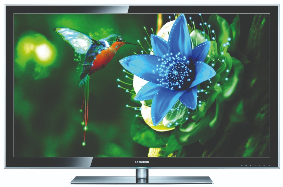
Samsung and Sony pioneered LED-backlit TVs. Launched in 2004 and costing many thousands of dollars, initial sales were sluggish. Thanks to a tremendous reduction in the cost of these screens, they are the incumbent technology today.
2005: The quest for ultra-efficient lasers
There’s an elegance in using a high-power laser to destroy tanks and missiles with a burst of incredibly powerful light. But even today, despite research and development into laser-based weapons going back 60 years, this idea is still a long way off becoming a mainstream military technology. There are various issues, including a phenomenon known as thermal blooming – it is a defocusing of the laser beam, caused by the creation of a plasma at very high levels of light intensity. Unfortunately, blooming is exacerbated by fog, smoke, dust and rain, none of which are strangers to the battlefield.
Despite all these concerns, in 2003 the US agency DARPA ran a three-year programme called SHEDS – super-high efficiency diodes sources – aimed at preparing the way for a laser-based weapon. This effort focused on propelling the wall-plug efficiency of commercial infrared laser bars from well below 50 percent to at least 80 percent. Hitting this target could lead to a highly-efficient 100 kW laser-based defence weapon, according to the sponsor.
Three US chipmakers took on the laser diode efficiency challenge: Alfalight, nLight and JDSU. All sailed past the 65 percent intermediate goal by refining their devices through initiatives that included the compositional grading of quantum-well interfaces, the introduction of materials that enhanced optical and electrical confinement, and changes to doping that cut contact resistance. But none could scale the dizzy heights to fulfil the final target, an efficiency of 80 percent.
Despite this failure, the programme has left a great legacy. And like many DARPA initiatives, the beneficiaries lie outside the military. Even in 2005, before the programme had finished, gains in laser efficiency were making an impact in industries that used solid-state, diode-pumped lasers for a wide variety of processing-related tasks, from shaping medical devices to welding car-body parts. Higher efficiencies were trimming the dollar-per-Watt metric, and in turn reducing expenditure on diodes that could total a third of the system cost. What’s more, device reliability improved, because greater efficiency meant less heat, and chips that run at lower temperatures.
Improvements to the diode’s bang-per-buck have also been instrumental in the success of fibre lasers. Offering a simple solution to the tricky problem of how best to focus light onto a target, diode-pumped fibre lasers are now widely deployed for cutting, welding, and folding of metals and polymers, with sales netting $3 billion per year.

Efforts to turn the vision of laser-based weapons into reality were supported by a DARPA-funded programme aimed at increasing the efficiency of infrared laser diodes from below 50 percent to 80 percent or more.
2006: Lighting up silicon
Silicon photonics sounds too great to be true. Whizzing photons around miniature racetracks in silicon chips churned out in state-of-the-art fabs promises a future offering affordable, breath-taking computational powers and superfast communication. But I know that you’ll have your doubts, because you know that silicon can’t emit light. That makes the manufacture of photonic chips quite a challenge.
If you want your light source on the chip, you’ll need to find a way to unite a III-V laser with a silicon waveguide while combatting problems arising from the significant lattice mismatch between these materials.
The first significant success in this endeavour came in 2006, through a partnership between engineers at Intel and John Bower’s group at the University of California, Santa Barbara. Using a low-temperature oxygen plasma, these researchers created a thin oxide layer on the surface of both materials. This layer enabled the fusing of an InP-based chip, containing AlGaInAs quantum wells, to the silicon waveguide strip, to create an electrically pumped laser. And due to the excellent coupling between these entities, the silicon waveguide played a fundamental role in the lasing action.
Building on this triumph, Intel had developed and commercialised a portfolio of transceiver products.
In 2016, it introduced a silicon photonics transceiver that supports 100G communications, and two years on, the company targeted 5G wireless front-haul applications with this product. This 100G transceiver has a transmitter and a receiver block, each with several die. The transmitter contains several InP lasers and a Mach-Zehnder modulator that encodes their signals, and the receiver features four germanium photodiode dies and a trans-impedance amplifier circuit.
Intel has now shipped more than 3 million 100G pluggable transceivers based on its silicon photonics platform, and demonstrated a four-channel device operating at 400 Gbit/s.
Intel has pioneered the integration of InP-lasers and silicon photonics. In this 50 Gbit/s link, the transmit module (left) sends laser light from the silicon chip at the centre of the green board, which travels through optical fibre to the receiver module (right), where a second silicon chip detects the data on the laser and coverts it back into an electrical signal.
2007: Debating droop
Some scientific questions pique interest but actually don’t matter that much because they are only of academic interest. But in 2007, that was certainly not the case for droop. Back then this mysterious malady pegged back the efficiency of LEDs at the current densities needed to win business in the biggest market of all, general lighting.
At that point in time researchers had ruled out heating as the cause and dismissed indium clustering, attributed as a measurement artefact. The search continued, with much riding on success. Unmasking droop would offer insight into how to build efficient devices that could light our homes and offices.
In February Philips Lumileds came out with a stunning, bold claim, saying that it had ‘fundamentally solved’ the problem of droop. According to this Californian chipmaker, LEDs that were free from this malady would follow in a matter of months.
Rather tantalisingly, the company offered no details of the cause of this deficiency. But in September they spilt the beans at the biggest nitride conference of the year. At a buzzing International Conference on Nitride Semiconductors, held in the heart of Las Vegas, Mike Krames, at the time the leader of the company’s Advanced Laboratories, unveiled Auger recombination as the cause.
The claim drew a mixed reception. Partly, it is a cause no-one wanted, because it fails to offer a route to making droop-free devices. Auger recombination is an intrinsic process that depends on the carrier density, and all that can be done to reduce it is a form of social distancing at the atomic scale, such as a widening of the wells. But in practice it’s very difficult to produce thick, high-quality quantum wells, due to strain.
What’s more, not all researchers agreed with Krames and his co-workers.
Some questioned the magnitude of the Auger coefficient required for this to be the primary loss mechanism, while others argued that just because it’s possible to fit a curve to a graph with a cubed dependence classically associated with Auger recombination, that is not proof that Auger causes droop.
An alternative theory came from Fred Schubert’s group and Rensselaer Polytechnic Institute in Troy, NY, working in partnership with researchers at Samsung and Joachim Piprek, a theorist at the device simulation consultancy NUSOD. This team, which started publishing papers in late 2007, attributed droop to carrier leakage. They went on to build polarisation-matched devices delivering higher efficiencies at higher drive currents.
The debate on the cause of droop raged for many years. In 2013, as we shall soon see, independent work laid claims of a smoking gun, providing definitive proof that Auger recombination is the cause of droop. But even that did not convince everyone.
2008: Sunny times
After many years of waiting, in 2008 the concentrating photovoltaic (CPV) industry looked like it would finally hit the big time. Venture capitalists had tired of investing in the telecommunication market and were starting to pour cash into cleantech, including developers of CPV, helping a handful of CPV companies to win contracts for multi-megawatt deployments. This led two makers of multi-junction cells – Spectrolab and Emcore – to fill up their order books. And competition for sales of these devices would soon increase, as the likes of Spire Semiconductors, MicroLink and Kopin prepared to launch rival products.
It had taken a long, long time for the fledgling CPV industry to get this far. The idea of focusing sunlight on highly efficient III-V cells can be traced back as far the late 1970s. A few years on from then a prototype had been put together by researchers at the Ioffe Physico-Technial Institute in St. Petersburg, Russia. Their system, reported in 1981 in a paper co-authored by Nobel-prize winning physicist Zhores Alferov, used reflectors as big as bin lids to direct sunlight onto 1.7 cm diameter AlGaAs/GaAs solar cells, butted up against aluminium pipes to prevent overheating. In the decades that followed, more demonstrators were put together, III-V cell efficiencies climbed and systems were built and sold, culminating in the deployment of a few tens of megawatts in the run up to 2008.
That year, market analyst Lux Research claimed that the long-term signs were great, with expenditure on installations employing III-V solar cells set to total $1.2 billion by 2012. Lux warned that some CPV start-ups would not survive, because they were failing to tackle important engineering issues surrounding maintenance, cooling and wind resistance. But that did not cause much alarm, as in an emerging market some firms will always go to the wall.
The unfortunate reality is that come 2012, the CPV industry was in tatters. Many firms had gone bust, while those that were left were on their last legs. The credit crunch, caused by a global economic crisis, starved these firms of investment crucial to increasing their size and delivering economies of scale. Another hammer-blow came from falling prices of silicon solar cells at the start of the last decade. Despite $500 million of investment, roughly just 100 MW of CPV has been deployed, with a lack of business bringing the demise of many big names in the sector, including Ammonix, SolFocus, Isofotón, GreenVolts and Semprius.
Today CPV is still down, but not quite out. In 2017, STACE, a supplier of electrical equipment in the power generation industry, bought the CPV assets of Soitec. Using this technology, which can be traced back to Concentrix, eight 30 kW CPV systems have been installed at the University of Sherbrooke, Quebec.
So, if further research into CPV allows it to become competitive enough to take on the incumbent – and that is definitely a big if – there is a company well-positioned to roll out this technology.

Interest in concentrating photovoltaics reached an all-time high in 2008. A leader in this field, Concentrix, used Fresnel lens to concentrate sunlight by a factor of typically 500 on triple-junction cells. A credit crunch and a dramatic reduction in the price of silicon PV wrought havoc in the fledgling CPV industry. Soitec purchased Concentrix in 2009, and then sold this technology to STACE, Canada, in 2015.
2009: Going green
What is easier – using an efficient blue LED as a starting point to build a laser emitting in the same spectral range; or starting with a laser that emits in the blue-violet, and constructing a variant that emits in the green? You would think it would be the later. After all, to go from an LED to a laser you need to introduce optical confinement, create mirrors, crank up the local carrier concentration and slash the defect density in the active region. In comparison, to turn a blue-violet laser into a green one, all you need to do is add a little more indium into the quantum well.
But if you take a look in the history books, you’ll reach a very different conclusion. Courtesy of Shuji Nakamura’s pioneering work, Nichia reported the first efficient blue LED in 1993 and took just two years to follow it up with a laser. But nearly another 15 years elapsed before the world had made its first green GaN laser.
The first important step towards this source came in 2003, with Nichia’s report of a 480 nm laser – still blue, but leaning to the green. Five years on, it had only advanced another 8 nm. Had this device come up against an invisible wall, with blue-green being the limit?
Any chances of getting to true green, considered to be 520 nm and beyond, seemed to rely on a radical re-design. To reach longer wavelengths requires a cranking up of the indium content, realised by lowering the growth temperature in the MOCVD chamber. But this riddles the device with defects, degrading light emission. Compounding the problem, intrinsic electric fields in these heterostructures pull apart electrons and holes in the wells, and as the indium content increases, they get even stronger. While these fields are beneficial on one hand, pushing emission to longer wavelengths, they make it harder to inject carriers into the device. Turning up the voltage forces them through, but negates the benefit of the internal field, so it’s goodbye to longer wavelengths.
A novel way to overcome this issue is to switch growth planes. Growing the device on the non-polar plane quashes the electric field. In early 2007, a team at the University of California, Santa Barbara, that included Nakamura – he joined this group from Nichia in late 1999 – did just that. They unveiled the world’s first non-polar laser, emitting in pulse mode at 404 nm.
The joy of leading the way didn’t last long. Just three days later Rohm reported a non-polar laser, this time operating in continuous-wave mode. When Rohm reached this milestone, it also set out its true ambition: building a 532 nm laser for colour displays. Before the year was out, it had stretched emission to 459 nm. Although Rohm then lost the lead when Sharp entered the fray in 2008 with a 463 nm non-polar laser, it retaliated with a 481 nm device.
2009 proved a pivotal year. In February Rohm revealed yet more progress, reaching 499.8 nm and eclipsing the best mark for conventional nitride lasers. At that point, a non-polar laser would have been the bookies’ favourite in the race for the first GaN green laser. But anyone thinking along those lines got an almighty shock nine days later, when a conventional laser took the lead. This didn’t come out of the labs of Nichia, but from a very dark horse – Osram Opto Semiconductors of Regensburg, Germany, which hit 500 nm by making ground on many fronts. Then, in the spring, Nichia grabbed the record, again with a conventional laser. It first reported success at 510 nm, before revealing it had made a 515 nm laser. How did it do it? It’s hard to tell – all the company would say is that it had improved the quality of its active region.
The first true-green laser came in summer 2009. Snatching the crown came GaN substrate specialist Sumitomo, announcing on 16 July a device emitting at 531 nm. Success came from a halfway house – that is, a semi-polar plane. This orientation quashes internal electric fields while providing a great foundation for growing indium-rich InGaN layers.
Further work has followed on non-polar, semi-polar and conventional planes. Last summer Sony reported a 525 nm semi-polar laser capable of an output of up to 1.75 W. And at this year’s Photonics West, Nichia revealed that it could do even better, having made a conventional 525 nm laser emitting up to almost 2 W. Such impressive results are helping to drive sales of green GaN lasers.
2010: The long-awaited transistor
Infineon’s launch of the world’s first SiC Schottky barrier diode in 2001 gave designers of power electronics a far more efficient device for controlling current flow.
However, while this wide bandgap diode helped to trim losses, circuit designers knew that they could do so much better if they could pair it with a SiC transistor, as that would improve the efficiency for turning currents on and off.
Start-ups and established makers of SiC devices took on this challenge. US outfit SemiSouth got their first, bringing to market a JFET in 2008. And within a few months, an alternative appeared: the BJT, launched by TranSiC, a spin-off of KTH Royal Institute of Technology Sweden.
But neither of these classes of SiC transistor won favour with designers. Both offered fast switching and a low on-resistance, hallmarks of SiC, but were ‘normally-on’. That’s a massive concern from a safety perspective. Although it’s possible to create a normally-off hybrid by adding another device, that’s an ugly solution.
Designers craved a more efficient, drop-in replacement for the silicon IGBT.
The SiC MOSFET ticks both these boxes, but it is very challenging to produce. One difficulty, taking many years to solve, is how to make a high-quality native oxide. This is a crucial layer that lies at the heart of the device, sitting between SiC and the metal contact. Engineers had no luck with any of the tricks employed in the silicon industry, so they had to find an alternative approach, such as a thermal growth process. A low channel mobility also applied the brakes to commercialisation, addressed by annealing in nitrogen gas, a step that slashes interface states.
By 2010, two of the biggest hitters in the SiC industry started to mass produce SiC MOSFETs. Which company won this race is a moot point to this day – both claim victory. The launch did not open the flood gates, with sales held back by high prices.
For example, not long after its launch, Cree’s MOSFET, sold through Digikey, retailed for $80 or more. Since then prices have fallen, while the number of producers has increased, now including STMicrolectronics and Mitsubishi. There is also more choice in blocking voltage and current handling, thanks to expanded portfolios and improved performance.
This summer Rohm launched its fourth generation of SiC MOSFET, while Cree has expanded its portfolio to over a dozen third-generation variants. All this activity is swelling sales, with SiC MOSFETs netting $85 million this year and expected to hit $348 million in 2025, according to market analyst Ahmed Ben Slimane from Yole Développement.
2011: A prize-winning bulb
In the not-too-distant past, many of us would agonise over what to do when our lightbulb failed and we had to replace it. If trimming carbon footprints topped our agenda, we would select a compact fluorescent. But they were never a hit. After installing one and flicking a switch, this bulb would take a minute or so to reach full brightness, by which time the room had been cast in a rather harsh light. Dimmer switches could not dial back the intensity, and when it came to disposal, care had to be taken with this mercury-ridden source.
If all those compromises were too much for us, we’d buy the well-established filament-based incandescent. It generated far more heat than light, and it didn’t last that long – 1,000 hours is typical – but it had many fans, as it instantly bathed the room with a lovely shade of white, and could be dimmed right down. Recognising these concerns and trying to do something about them, the US Department of Energy launched a competition in 2008 called the Bright Tomorrow Lighting Prize, better known as the L-Prize. $10 million were up for grabs, awarded to the first company that produced a bulb that combined the virtues of an incandescent with running costs that bettered a compact fluorescent and an incredibly long lifetime.
In August 2011 Philips claimed victory with a dimmable bulb that drew just 9.7 W while putting out its peak output of 910 lumens – that is 110 lumens more than a typical 60 W incandescent. Philips’ bulb underwent a range of tests to evaluate robustness, including being shaken, operated in temperature extremes and high levels of humidity, and driven with an imperfect voltage supply. Passing all evaluations with ease, it offered a lifetime of 25,000 hours, more than double that of a compact fluorescent.
When Philips launched this most impressive of sources it commanded a price so high that it would put off many early adopters. Would anyone really be willing to spend $50 on a single bulb? Fortunately, prices have plummeted over the last few years. Today, if you shell out $50 on solid-state lighting, you could return from a hardware store with a score of Philips’ 60 W-equivalent LED bulbs. Thanks to these competitive prices, many homes are now lit by a collection of light-emitting chips.
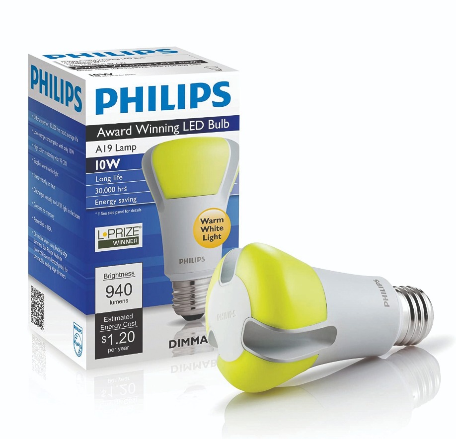
The 60 W incandescent bulb has many great attributes: instant on, a nice warm hue, and the opportunity to dim output. The $10 million L-Prize challenged makers of LED bulbs to replicate all these merits, while drawing less than 10 W. Philips Lumileds got their first, before launching their award-winning bulb. One striking feature of this award-winning source is the yellow colour of its emitting surface, easily visible when the bulb is not on. The yellow is associated with the remote phosphor, which when pumped with a battalion of 18 LEDs, casts a room in uniform, warm shade of white light.
2012: Gallium nitride gets its credentials
Hero results pique interest but don’t guarantee sales. That’s because designers want products that combine a great performance with longevity.
Developers at Transphorm understood this completely. They knew their GaN FETs were attracting much attention because they were a promising product, exceeding the efficiency of silicon and coping far better at elevated temperatures. However, to win sales, Transphorm had to assure potential customers that they should not have any concerns over reliability, so they put this 600 V FET in for independent device testing. This device passed to give Transphorm, in 2012, the industry’s first GaN FET qualified to the JEDEC standard.
Initial products by this West-coast firm were produced on SiC substrates. But production soon switched to silicon. Merits of this move were not limited to a cheaper, larger foundation, but included the opportunity to process devices on mature 200 mm lines, potentially in under-utilised fabs.
Efforts at proving device reliability continue. Transphorm’s GaN-on-silicon FETs are now qualified at standard temperatures and 175 °C, helping to drive sales, which surpassed 500,000 last November. Fourth-generation products launched this April have taken performance of GaN-on-silicon FETs to a new high and helped increase penetration into markets that include power supplies for computers and passenger planes, servo motors, and electric-vehicle on-board chargers.
2013: Droop’s smoking gun?
Would it ever be possible to draw the debate on droop to a close? Given the competing, vigorously defended theories, it would require irrefutable proof. Obtaining this would not be easy, but in Spring 2013 claims of a smoking gun surfaced from a partnership between researchers at the University of California, Santa Barbara (UCSB), and the École Polytechnique in France.
This team’s evidence came from an extremely elegant experiment that drew parallels with that made by Robert Millikan at the start of the twentieth century. Millikan studied the photoelectric effect by measuring the kinetic energy of electrons exiting a metal bombarded with beams of photons.
On this more recent occasion researchers injected carriers into the quantum well and recorded two phenomena: the light emitted by the LED, and the energy of electrons exiting through the p-side of the device. To ensure all thermalised electrons left the LED, the p-side surface had been treated with caesium.
As the scientists from this collaboration cranked up the current through their device, they detected higher energy peaks, associated with the vacuum-emitted electrons. According to them, this observation provided unquestionable proof that Auger is the cause of droop. In their view, no other mechanism could be responsible for these ‘hot’ electron peaks. Strengthening this claim, they found that when droop kicked in, high energy peaks started to emerge.
So, did other researchers working in this field raise a glass, toast this team’s success and agree that this work had put the debate on droop to bed? Absolutely not. In general, those that are trying to fathom the cause of droop have entrenched positions and are convinced that after examining all the evidence the theory they postulated is still the most convincing.
Critics argued that the experimental results may have been interpreted incorrectly. Boston University’s Enrico Bellotti claimed that the experiment suggests that electron leakage is the cause of droop, with some help from the Auger effect.
Fred Schubert from Rensselaer Polytechnic Institute in Troy, NY, tended to agree, suggesting that some electrons detected in the experiment might not be associated with the Auger effect at all, having simply leaked out of the LED’s quantum well. Another reason why Schubert struggles to view Auger recombination as a major contributor to droop is that he considers droop to be stronger at low temperatures, while Auger is weaker.
The team from UCSB and the École Polytechnique addressed their critics in the November & December 2013 edition of Compound Semiconductor magazine. In their feature, they argued that in their LEDs, the electric field is not strong enough to cause electron leakage. They also countered claims that it would not be possible to observe Auger-generated electrons escaping into vacuum, and expressed concerns related to a claim that free-carrier absorption could be a cause of droop.
Discussing competing theories will have helped to progress efforts to come to a consensus on the cause of droop. But even now, the debate has not completely disappeared.
By tracking the energy of non-radiative electrons that pass through an LED while simultaneously recording the light output of this device, researchers from the University of California, Santa Barbara, and the École Polytechnique, France, claimed they had definitive proof that Auger is the cause of droop.
2014: A full complement
The prospects of emerging devices can be judged by the actions of the biggest players manufacturing products with the incumbent technology. If alternatives have an outside chance of success, a few leading firms might dabble in them; and if they are certain to play a major role, multi-nationals will invest, either through acquisitions or internal development.
Judged in this manner, wide bandgap technology is assured of an important role in the future. All the leading firms in the power electronics sector have branched out from considering only silicon devices, and made headway with either SiC or GaN.
In the case of Infineon, it’s not hedging its bets as to which of these two rivals is going to play a bigger role. Instead, it is pursuing both, viewing GaN as a strong candidate for below 600 V and SiC as the best option for higher voltages. Infineon did not embark on an internal development programme for GaN, instead deciding to acquire this technology. In 2014, it agreed to shell out $3 billion in cash for GaN-on-silicon pioneer International Rectifier (IR). Note, however, that as well as gaining IR’s GaN-based technology, it also picked up its low-voltage silicon MOSFET family, which accounted for the lion’s share of sales. When Infineon took IR into its fold, it viewed GaN-on-silicon as a long-term investment, generating sales at least five years down the line.
In March 2015, Infineon deepened its involvement in GaN, teaming up with Panasonic. This duo signed a deal committing them to jointly develop devices that combined Panasonic’s normally-off GaN-on-silicon transistors with Infineon’s surface-mounted packages that would house these chips.
More recently, Infineon has broadened its portfolio of CoolGaN products, made using its own devices. So GaN is underway and SiC and silicon are well established, giving this German powerhouse an incredibly broad portfolio.
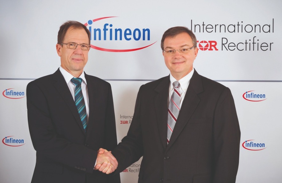
In 2014, Infineon agreed to purchase International Rectifier for $3 billion. Orchestrators of the deal were Reinhard Ploss (left), CEO of Infineon Technologies, and Oleg Khaykin (right), President and CEO of International Rectifier.
2015: Two titans unite
During the last 25 years, the two biggest sectors within our industry have headed in very different directions. In the late 1990s five LED chipmakers rose to the fore – Nichia, Cree, Lumileds, Toyoda Gosei and Osram – and all have held on to one of these top spots for many years. Today they are still active, shipping high volumes, but their collective share is in decline, now accounting for less than half of the $20 billion LED chip market.
In stark contrast, the GaAs microelectronics industry, second in revenue to only the LED sector, has seen a dramatic contraction in the number of competitors, despite a growth in revenue over the last 25 years from below $0.5 billion to around $8 billion.
Big players that have left this industry include Anadigics, snapped up in 2016 by II-VI after spending its last few years converting its RF line to the production of VCSELs. Other leading names have merged.
In 2002, Skyworks formed through the marriage of Alpha Industries and Conexant, and more recently Qorvo emerged from the union of two heavyweights, RFMD and TriQuint. This new entity started trading on 1 January, 2015.
That merger had much going for it. Many viewed the two companies as complementary, with RFMD having greater strength in RF technologies for handsets and TriQuint offering a better portfolio of defence products.
Investors clearly approved of the union, with the share prices of both firms enjoying double-digit jumps on disclosure of the plans.
The new entity had the potential to net an annual revenue of just over $2 billion; and thanks to synergies providing yearly savings of $150 million, gross and operating margins were tipped to be 45 percent and 25 percent, respectively.
Five years on, has the merger delivered on all those promises? Well, sales for fiscal 2020, finishing on 28 March of this year, amassed $3.24 billion, with gross and operating margins of 41 percent and 13 percent, respectively.
So sales are well above those expected in 2015, while margins are healthy, but not as high as hoped. Investors seem content with these figures – Qorvo’s share price is now just north of $110, up from $70, the value of this stock on its first day of trading.
2016: True heavyweight flexes its muscles
If you are a regular reader of this magazine, then by the middle of the last decade you would have been aware of the tremendous promise of gallium oxide. With a whopping bandgap of around 5 eV – the precise value depends on the particular polytype – it has the potential to deliver a knockout blow to those two blossoming middleweights, SiC and GaN.
Thanks to gallium oxide’s far wider bandgap it should be able to reign supreme in that most valued of characteristics, the on-resistance as a function of breakdown voltage. But that’s not its only alluring attribute: it offers versatility, because a thin film of gallium oxide can be deposited by a variety of techniques, including MBE and MOCVD; and there are several options for the substrate. Devices can be grown on sapphire or on gallium oxide, which could tumble in price, because boules of this material can be produced by melt-based techniques.
Gallium oxide’s great promise has had no trouble in attracting interest and initial investment. However, like any material, its first steps towards commercialisation hinged on demonstrations of device capability. They came thick and fast in 2016.
During that year two key breakthroughs emerged from a team at the Air Force Research Labs (ARFL). Using structures made from the β-polytype and grown on a native substrate, engineers working there grabbed the limelight by producing a MOSFET with a record-breaking critical field strength of 3.8 MV/cm – that’s about four times the critical field strength of GaN. And later that year they realised another breakthrough, reporting the first ever enhancement-mode FET with a high-breakdown voltage in the off-state. This second success demonstrated that a lack of p-type carriers in gallium oxide is not a show-stopper to making a normally-off FET.
The gallium oxide research programme at ARFL had been inspired by the work at Japan’s National Institute of Information and Communications (NICT). Researchers at NICT, working with domestic partners, had driven much early progress in both materials and devices, and gone on to produce the world’s first MESFETs and MOSFETs in 2012.
Four years down the line refinements to NICT’s MOSFET, which included the addition of a field plate, had bolstered the breakdown voltage to just over 750 V, a result that is still impressive today.
Japan also provided another milestone in gallium oxide. In 2016, using a novel growth technique known as mist epitaxy, researchers at Flosfia reported a-Ga2O3-on-sapphire Schottky barrier diodes sporting an on-resistance that trumps state-of-the-art variants made from SiC. This spin-off of the University of Kyoto is commercialising these ultra-wide bandgap diodes, along with accompanying MOSFETs. Production ramps are slated for this year.
2017: Creating the world’s first compound semiconductor cluster
What is the most famous valley in the world? OK, it might not be the first answer to trip off your tongue, but a great case can be made for Silicon Valley.
While this region may not have that many fabs today, the engineers that worked here – many of them graduates of Stanford University – are to be thanked not only for their advances in technology, but for giving all of us that work in the semiconductor industry a higher status in society. Today technology is admired, benefitting many, even if the average man in the street has never heard of holes, bandgaps or lithography.
California is not the only part of the world with a cluster of semiconductor companies. They are also found in Leuven, Belgium; in Dresden, Germany; in Eindhoven, The Netherlands; and in Grenoble, France. Together, clusters comprise 800 companies and account for 150,000 jobs. By having many firms nearby, often operating at different positions within the supply chain, they support one another while attracting more engineering talent to the region. This helps to increase the kudos of the clusters, bringing in yet more business and innovation, while fostering an entrepreneurial outlook that gives local start-ups the best chance of thriving.
Efforts to create the world’s first compound semiconductor cluster can be traced back to 2011, when IQE’s charismatic leader, Drew Nelson, met the economic minister for Wales at that time. Nelson put the case for a far stronger infrastructure within the UK to support the compound semiconductor industry. Back then, IQE had virtually no domestic customers. That’s not to say, however, that IQE was the only company in South Wales working in our industry: this part of the UK was and continues to be home to etching and deposition tool maker SPTS, and a Microsemi facility with packaging expertise.
Nelson’s next steps included working within a group set up by the European Commissioner for Technology for the Digital Economy. Involved in a team considering key enabling technologies, Nelson championed the construction of a sovereign capability for compound semiconductors in South Wales to rebuild the continent’s manufacturing capability for this technology.
Building on these efforts, Nelson lobbied the Welsh Government and Cardiff University to set up an Institute for Compound Semiconductors. He had a vision for a local facility, delivering cutting-edge technology, developed using tools and processes compatible with high-volume manufacturing. In March 2015 the UK Government funded this initiative, and a year on planners gave the go-ahead for the construction of a new building for the Institute for the Compound Semiconductors. Forming part of the new Innovation Campus, the Institute is slated to open late next year.
To help commercialise the technology developed at the Institute for Compound Semiconductors, in 2015 IQE and Cardiff University founded a joint venture: the Compound Semiconductor Centre. Using funding from Cardiff University and some equipment from IQE, it runs collaborative research projects.
In 2016 that year, more links were added to the supply chain. In January, the UK government stumped up £50 million, funding the creation of a Compound Semiconductor Catapult, an open access R&D facility focused on helping UK businesses exploit advances in compound semiconductor technologies. And later that year the UK’s Engineering and Physical Sciences Research Council poured £10 million into a Manufacturing Hub for Compound Semiconductors, targeting the translation of research into high-volume chip manufacturing.
With many pieces of the jigsaw now in place, in summer 2017 the cluster officially opened for business, taking the name CSconnected and holding events with speakers from all key stakeholders. The cluster also took a huge leap forward, grabbing an opportunity to get its hand on a production line. The 200 mm silicon fab in Newport, South Wales, had come into the hands of Infineon through its acquisition of International Rectifier. After the German powerhouse evaluated its global chip manufacturing capabilities, it viewed the Newport Fab as surplus to requirements. This facility was put up for sale, with Nelson leading a private equity buyout. Emerging from this deal, Newport Wafer Fab had guaranteed orders from Infineon for two years.
Further ahead, those in the cluster hoped that the lines would also be used to produce compound-semiconductor-on-silicon chips. This fab has a track record in processing GaN-on-silicon devices, produced during International Rectifier’s tenure, but other material systems are possible. Such efforts will be aided by IQE’s acquisition of Translucent, a developer of rare-earth oxides, which can provide a bridge between a silicon wafer and compound semiconductor epilayers.
Those within CSconnected are continuing to advance. The CS Catapult has moved into part of a very large building constructed for LG Semicon, with IQE taking the remainder, using it to create an epifoundry that could house up to 100 MOCVD tools. The cluster has also expanded to include Swansea University, which is constructing a Centre for Integrative Semiconductor Materials. Such activities will continue to create job opportunities and swell revenues. According to a report published last August by Cardiff University, the cluster now accounts for more than £460 million in sales and nearly 1500 jobs. That’s a good start towards a very long-term goal of eventually creating 5,000 positions in the compound semiconductor industry.

Construction of the Institute for Compound Semiconductors is well under way, and should be completed next year.
CSconnected, the world’s first compound semiconductor cluster, opened for business in 2017. By the end of the year this cluster, based in South Wales, had strengthened its capabilities, thanks to the launch of Newport Wafer fab, a facility Infineon deemed surplus to its requirements.
2018: Getting the blues
The VCSEL has some wonderful strengths. It is efficient, allowing it to run off a battery; it can be turned on and off at very high speeds, making it a great source for transmitting vast amounts of data; by adjusting the size of the aperture, it allows single-mode emission with a circular profile, simplifying optics; and it is well-suited to high-volume manufacturing, partly because its design allows on-wafer testing.
However, there is room for improvement. Despite decades of development, the VCSEL spans a far narrower range of wavelengths than edge-emitting lasers and LEDs. Expansion of the spectral domain has been very slow, given the long history of this device. Its roots go back as far as 1965, when Ivars Melngailis, working in the MIT Lincoln Lab, announced a ‘longitudinal injection laser’ emitting at 5.2 μm. This device, formed from an InSb diode and featuring polished top and bottom surfaces to ensure optical feedback, was incredibly impressive feat for its time, but is far from practical. Lasing required a hefty 20 A drive current and cooling to 10K.
The first real VCSELs came from the labs of Kenicha Iga from Tokyo Institute of Technology. In 1977, Iga proposed a design that shares many of the features of today’s VCSEL. For the next 11 years he almost singlehandedly pioneered this class of device, before other groups noted his breakthrough and redirected their efforts towards this technology. Success followed, with research in the latter part of the twentieth century initially focusing on the near infrared, before attempts were made to widen the spectral range of the VCSEL in both directions.
Initially, breakthroughs with the GaAs-based material system enabled 850 nm and 980 nm VCSELs, before further progress stretched emission to around 650 nm. Wafer-fusion brought yet more success, allowing GaAs-based mirrors to be united with InP-based active regions to realise emission at 1.5 μm.
By the turn of the millennium, researchers started to consider the next goal: expanding emission to the blue and green. Success would open up new markets, allowing devices to be deployed for high-resolution printing, high-density optical data storage, chemical and biological sensing, full-colour displays and lighting.
Producing VCSELs operating in this spectral domain is far from easy. To reach these shorter wavelengths, the GaAs-based material system has to be replaced with one based on GaN and its related alloys. The switch may sound a simple, but it’s anything but.
The biggest issue is producing the mirrors that sit either side of the active region. This is relatively easy in a GaAs-based VCSEL, because this material system is blessed with the pairing of GaAs and AlGaAs. These III-Vs have very similar lattice constants, so strain is not an issue, and there is a significant difference in their refractive index, aiding reflection. When 20 pairs of alternating layers of GaAs and AlGaAs make a mirror, it has a reflectivity of 99 percent, sufficient to make a high-performance VCSEL.
For blue and green VCSELs, to prevent strain from degrading the mirrors, GaN has to be paired with Al0.83In0.17N, a trickier alloy to grow that has a relatively low refractive index contrast. Growing two sets of GaN-based mirrors takes too long, so it is better to combine a nitride-based bottom mirror with a top one based on dielectrics, an approach pioneered by Nicholas Grandjean’s team at EPFL. Their high-point came in 2007 when they reported the first optically pumped GaN VCSEL. Frustratingly, funding dried up for Grandjean, with those holding the purse strings arguing that the first electrical GaN VCSEL would come from Japan. They were more or less right, and now we will never know if Europe could have beaten them to it.
The first GaN VCSEL actually came from National Chiao Tung University, Taiwan, announced in April 2008. This device required cryogenic cooling, a restraint overcome later that year by Nichia, using a pair of dielectric mirrors. Nichia persisted with this design, increasing the output power to 0.62 mW in 2009, before making further minor but additional gains. But the lack of substantial progress appears to have curtailed further GaN VCSEL development by the Japanese chipmaker. Nichia never came close to 10 mW, the ballpark figure for augmented-reality devices, projection systems and displays. That milestone came in 2018, achieved by two Japanese companies working independently. Stanley Electric, partnering with Tetsuya Takeuchi and his team from Meijo University, built on the work at EPFL, improving the growth conditions. In the autumn of that year they reported a blue VCSEL with an output in excess of 15 mW. And in November 2018, Sony unveiled a 12 mW VCSEL with a novel design, featuring a far larger cavity that incorporated a thinned GaN substrate, and a curved mirror grown on the backside of the wafer.
Alongside these breakthroughs in blue VCSEL performance, 2018 will be remembered for the market success of the infrared cousins. Up until then, datacoms provided by the primary revenue stream for this device, but in 2018 the market for handsets caught up, according to Pierrick Boulay, Technology and Market Analyst at Yole Développement.
A year before, Apple had launched iPhones incorporating VCSEL-based sensing, and in 2018 it became the main consumer of these lasers in smartphones. Although VCSELs were also featuring in 2018 models made by Xiaomi, Vivo, Huawei and Oppo, they were far less popular with consumers. Initially, Apple bought its VCSELs from Lumentum. But in late 2017 the technology giant decided that it needed to secure a second source, so dangled a carrot at Finisar, promising orders for $390 million of VCSEL products. Qualifying this device took time and did not dent Lumentum’s orderbook in 2018.
Boulay predicts strong growth for VCSELs, as they will see increasing use in smartphones, continued deployment in datacom networks, and start to feature in sensing applications covering greater distances, such as automotive LiDAR. The market for these surface-emitting lasers is expected to mushroom from $738 million in 2018 to $3.7 billion in 2024.

Facial recognition offers a lucrative market for the infrared VCSEL.
To secure a second source for VCSELs, Apple agreed to purchase $390 million of these devices from Finisar.
2019: A monumentous cash injection for silicon carbide
In spring 2019, Cree, the developer of SiC substrates and various optoelectronic, RF and power devices, re-aligned its business in emphatic fashion. It’s relatively new CEO Greg Lowe had no qualms in carving off the company’s Lighting Products division to Ideal Industries; giving the LED business that brought so many years of success a back seat; and focusing on wide bandgap materials and RF and power devices.
Helping to have made this monumental decision would have been a number of lucrative SiC wafer supply deals: contracts with Infineon, ST Microlectronics and other companies totalled $500 million.
By summer 2019 Cree’s LED business had softened and it had netted the lion’s share of its $310 million sale to Ideal. These circumstances would have helped Lowe to move forward with his vision, investing $1 billion in massive expansion of SiC capacity. A state-of-the-art, 200 mm facility would be built by 2024, delivering a 30-fold expansion in capacity compared with the first fiscal quarter 2017.
Later that year Cree had an offer it could not turn down – a $500 million grant from the state of New York. Instead of having to spend $450 million retrofitting an existing structure at its headquarters in Durham, NC, it could now invest $170 million in building a new, automotive-qualified 200 mm power and RF wafer fabrication plant in Marcy, New York.
The new building should be up and running in 2022, initially using 150 mm wafers before transitioning to 200 mm wafers two years’ later. Until that comes on line, capacity is being increased at the headquarters.
Since these announcements, the proportion of revenue coming from the less profitable LED products line has continued to decline, while that from the Wolfspeed division – it encompasses SiC wafers, power electronics and RF devices – has seen revenue grow. Sales are currently taking a knock from the Covid-19 epidemic and trading restrictions with China, but the long-term prospects for Cree are very, very good.

Supported by a $500 million grant from the state of New York, Cree/Wolfspeed, is building a new automotive-qualified 200 mm power and RF wafer fabrication plant in Marcy, New York, that should be up and running in 2022.
2020: The beginnings of a microLED display revolution
What will this year be remembered for? With several months still to go it’s not yet clear, but within our industry let’s certainly hope it’s not for Covid-19. Fabs are running, and while business is impacted, compared to many sectors of the economy we are relatively unscathed.
It’s quite possible that 2020 will go down in history as the year when microLED displays started to gain traction. Making them is not easy, as it tends to involve moving millions of micron-sized LED chips from their wafers to a display backplane, while ensuring zero duds. But these efforts are rewarded, with the resulting displays delivering ground-breaking brightness, incredible efficiencies, exceptional levels of contrast and freedom from burn-in.
A tremendous amount of money has already been pumped into microLED technology. According to
Yole Développement, funding to date totals $4.8 billion. Of that, Apple accounts for $1.8 billion, a figure that includes the Luxvue acquisition and internal development.
Facebook is another tech titan with ambitions of using microLEDs in its future products. It is partnering with Plessey, a UK company that has overcome issues of mass transfer by producing its LEDs on GaN-on-silicon wafers subsequently bonded to a silicon backplane. Making blue and green LEDs with GaN is well-known, while red is far more challenging. However, last December Plessey announced that through strain engineering it had realised red emission from this class of device, opening the door to a new way to make full-colour displays.
MicroLEDs also have opportunities outside of displays. This summer engineers at CEA-Leti have broken the record for data transmission for LiFI, using a 10 μm microLED to transmit at 7.7 Gbit/s. This method of transmission can guarantee secure communication within a room, a feature not offered by WiFi or 5G.
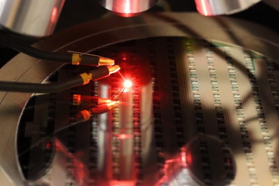
By straining its GaN-on-silicon LEDs, Plessey can produce red, green and blue emitters on the same wafer. This aids the creation of a full-colour microLED display, a technology that has enabled Plessey to team up with Facebook.


