
Adjusting the properties of 2D Semiconductors
Scientists experimentally realise 2D Si-Ge alloys with tuneable electronic properties
Scientists from Japan Advanced Institute of Science and Technology (JAIST) have realised the first experimental demonstration of the 2D alloy Si-Ge. They have also shown that the Si to Ge ratio can be adjusted to fine tune the electronic properties, paving the way for novel applications.Their study is published in Physical Review Materials.
2D semiconductor alloys are seen as a promising option to go past the technical limitations of modern electronics. Unfortunately, graphene, the carbon-based poster child for 2D materials, does not lend itself easily to alloying, which leaves it out of the equation.
However, there is an alternative: silicene. This material is composed entirely of silicon atoms arranged in a 2D honeycomb-like structure reminiscent of graphene. If the properties of silicene could be tuned as needed, the field of 2D silicon-based nanoelectronics would take off. Although alloying silicene with germanium was theoretically predicted to yield stable 2D structures with properties tuneable by the Si to Ge ratio, this was never realised in practice.
The JAIST team have have experimentally demonstrated a new way to grow a silicene layer and stably replace a portion of its atoms with Ge, allowing them to fine tune some of its electrical properties.
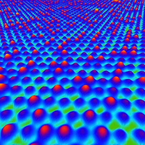
First, the scientists grew a single layer of 2D silicene onto a ZrB2 thin film. The ZrB2 was grown on a silicon substrate through the surface segregation of Si atoms which crystallise in a 2D honeycomb-like structure. However, this silicene layer was not perfectly flat; one sixth of all Si atoms were a bit higher than the rest, forming periodic bumps or 'protrusions.'
Then, Ge atoms were deposited onto the silicene layer in ultrahigh vacuum conditions. Interestingly, both theoretical calculations and experimental observations through microscopy and spectroscopy revealed that Ge atoms could only replace the protruding Si atoms. By adjusting the number of Ge atoms deposited, a Si-Ge alloy with a desired Si to Ge ratio could be produced. The composition of the final material would thus be Si6-xGex, where x can be any number between 0 and 1.
The team then studied the effects of this adjustable Si to Ge ratio on the electronic properties of the Si-Ge alloy. They found that its electronic band structure could be adjusted within a specific range by manipulating the composition of the material. Excited about the results, senior lecturer Antoine Fleurence from JAIST, lead author of the study, remarks: "Silicon and germanium are elements commonly used in the semiconductor industry, and we showed that it is possible to engineer the band structure of 2D Si-Ge alloys in a way reminiscent of that for bulk (3D) Si-Ge alloys used in various applications."
The implications of this study are important for multiple reasons. First, the ultimate thinness and flexibility of 2D materials is appealing for many applications because it means they could be more easily integrated in devices for daily life. Second, the results could pave the way to a breakthrough in electronics. Co-author of the study, Yukiko Yamada-Takamura from JAIST, explains: "Semiconducting 2D materials made of silicon and germanium with atomically-precise thickness could further decrease the dimensions of the elemental bricks of electronic devices. This would represent a technological milestone for silicon-based nanotechnologies."
'Band engineering in an epitaxial two-dimensional honeycomb Si6−xGex alloy' by A. Fleurence el al; Phys. Rev. Materials 5, L011001 21 January (2021)


