
Switching nanolight on and off
Columbia researchers discover a new way to program light on an ultra-small scale
A team of researchers led by Columbia University has developed a unique platform to program a 2D semiconductor WSe2, producing imaging capabilities beyond common limits on demand. The research appears Feb. 4 in the journal Science.
The discovery is an important step toward control of nanolight, which is light that can access the smallest length scales imaginable. The work also provides insights for the field of optical quantum information processing, which aims to solve difficult problems in computing and communications.
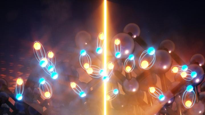
"We were able to use ultrafast nano-scale microscopy to discover a new way to control our crystals with light, turning elusive photonic properties on and off at will," said Aaron Sternbach, postdoctoral researcher at Columbia who is lead investigator on the study. "The effects are short-lived, only lasting for trillionths of one second, yet we are now able to observe these phenomena clearly."
Nature sets a limit on how tightly light can be focused. Even in microscopes, two different objects that are closer than this limit would appear to be one. But within a special class of layered crystalline materials--known as van de Waals crystals--these rules can, sometimes, be broken. In these special cases, light can be confined without any limit in these materials, making it possible to see even the smallest objects clearly.
In their experiments, the Columbia researchers studied the van der Waals crystal WSe2, which is of high interest for its potential integration in electronic and photonic technologies because its unique structure and strong interactions with light.
When the scientists illuminated the crystal with a pulse of light, they were able to change the crystal's electronic structure. The new structure, created by the optical-switching event, allowed something very uncommon to occur: Super-fine details, on the nanoscale, could be transported through the crystal and imaged on its surface.
The report demonstrates a new method to control the flow of light of nanolight. Optical manipulation on the nanoscale, or nanophotonics, has become a critical area of interest as researchers seek ways to meet the increasing demand for technologies that go well beyond what is possible with conventional photonics and electronics.
Dmitri Basov, Higgins professor of physics at Columbia University, and senior author on the paper, believes the team's findings will spark new areas of research in quantum matter.
"Laser pulses allowed us to create a new electronic state in this prototypical semiconductor, if only for a few picoseconds," he said. "This discovery puts us on track toward optically programmable quantum phases in new materials. "
'Programmable hyperbolic polaritons in van der Waals semiconductor' by A. J. Sternbach et al; Science 05 Feb 2021: Vol. 371, Issue 6529


