
Beneq ALD Enables Next-Generations of Power Devices
Driven by fast-growing demand in electric vehicles, consumer electronics and renewable electricity modern power devices are evolving rapidly in terms of materials as well as design and process technologies. For example, Wide Bandgap SiC and GaN devices have the fundamental advantage of low on-resistance x high breakdown voltage. Increasingly advanced deposition technologies are required across the board. The most critical are the dielectrics to be grown or deposited at the surface of the semiconductor, either as part of the active MOS or MIS structure or as a surface passivation layer.
ALD holds unique advantages over other deposition methods such as PECVD
- Unrivalled conformality, sub-nanometer thickness control and uniformity
- Broad range of materials, including Al2O3, AlN, HfO2, Ta2O5, SiO2, Si3N4, TiN, TiO2, ZnO, and metals etc.
- Greater electrical, morphological, optical, and mechanical tuneability
- High quality at low temperature - typically between 50–400 °C
Proprietary Beneq in-situ pre-clean and passivation is especially developed for metal and semiconductor surfaces – Silicon and compound semiconductor. In other words, ALD also differentiates by its capability to grow thin dielectrics of thermal quality at much lower temperature than thermal processes such as thermal oxidation. ALD enables low thermal budget process integration.
Not only SiC and GaN devices but also mainstream MOSFET’s and IGBT benefit from the above merits enabled by advanced integrated ALD technology.
Thanks to rapid advances in ALD equipment technology, throughput can now be scaled by using batch process i.e. 25 wafer batch as much as needed. Thermal batch ALD enables production-worthy throughputs (double digit) for thicknesses in the range of 10 to 100 nm.
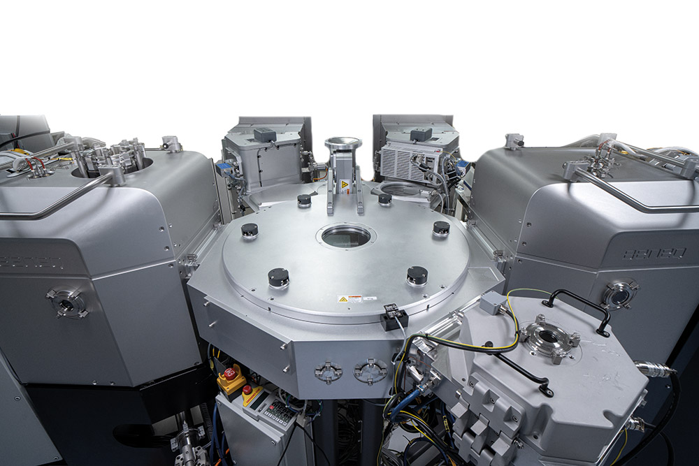
Beneq TransformTM cluster tool is a fully automated, in-vacuum cassette-to-cassette ALD manufacturing solution.
“The Beneq TransformTM mainframe is built on an industry-standard handling system, equipped with a four-sided – Beneq TransformTM Lite – or six-sided transfer module including one or two cassette load locks for production worthy reliable cassette-to-cassette full single wafer automation. The configuration is highly flexible and scalable and can be adapted to various R&D and manufacturing requirements for wafer sizes from 3’’ up to 8’’,” says Dr. Patrick Rabinzohn, Business Executive, Semiconductor ALD Business Line.

Beneq TransformTM platform overview © All rights reserved.
The Beneq TransformTM can be configured with or retrofitted with Beneq single wafer thermal and/or plasma as well as batch ALD process modules. Its proprietary preheating module nearly eliminates heating related waiting time, boosting productivity to a whole new level. In addition, the mainframe accommodates an optical aligner, and can be equipped with optional integrated Brooks TopCoolerTM cool-down unit, and internal wafer buffer. The Beneq TransformTM is fully compliant with ultra-clean requirements, SECS/GEM communication and SEMI S2 and S8 standards certified.
Designed with versatility at heart
Beneq TransformTM can be used to deposit a wide range of oxides, including Al2O3, HfO2, Ta2O5, TiO2 and SiO2 using thermal single wafer or batch ALD, and nitrides such as AlN, Si3N4 using plasma enhanced ALD. In addition to oxides, thermal batch processing up to 25 wafers for nitrides such as AIN and TiN requiring high processing temperatures is supported. Beneq TransformTM is the leading choice for all More-than-Moore applications. It is configured to have the smallest footprint and lowest cost-of-ownership for any of the very diverse process capabilities x capacity requirements of the MtM market segments shown below.

Beneq ALD solutions for More-than-Moore markets
Beneq TransformTM tool is fully upgradable in the field from 3” to 8’’ wafer processing. For both the single wafer / plasma enhanced ALD process module and the thermal batch ALD process module, a simple process kit change needs to be done.
Additionally, Beneq single wafer process module comes with high degree of built-in processing versatility, which is particularly beneficial in processing sensitive materials such as SiC, GaN, GaAs, and InP. Firstly, the plasma ALD module can be used for efficient in-situ surface pre-clean/nitridation, which is crucial for eliminating surface states associated with non-stoichiometric oxides. A further benefit is the capability of sequencing of plasma/thermal nitrides and thermal/plasma Oxide processes in the same chamber either as bi-layer or as laminates/mixtures, without the need to transfer the wafer from a nitride chamber to an oxide chamber. A further processing option is the possibility to switch the plasma enhanced ALD module to thermal ALD processing only, by a simple change kit. In a nutshell from single wafer and batch process modules to single wafer sequential and parallel processing versatility is at the heart of BENEQ Transform™.


