
Targeting telecoms with nanowires
Nanowire lasers could provide the telecom industry with a widely tuneable source that is easy to integrate with silicon photonics.
BY GUOQIANG ZHANG FROM NTT CORPORATION
ALMOST ALL DEVICES produced by our industry are formed from compound semiconductor heterostructures. By controlling the composition, doping and thickness of every layer within an epitaxial structure, we are able to produce a wide range of devices with excellent characteristics.
One such device is the edge-emitting InP-based laser. Generating sales of billions of dollars, this class of laser, which operates in the spectral domain spanning 1.2 µm to 1.6 µm, is a key ingredient in optical communication networks.
To produce these telecom lasers, engineers load InP substrates into MOCVD reactors and deposit an epitaxial stack containing layers of InP and InGaAs(P). It is a material combination that has its pros and cons – by adjusting the composition, the designer can adjust the wavelength of the laser’s emission, targeting absorption minima in optical fibres; but there are mismatches in lattice and thermal expansion coefficient between InP and its related alloys, and this hampers further integration into functional systems and platforms.
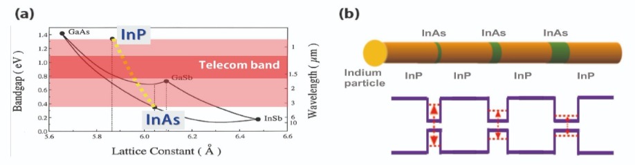
Figure 1. (a) Bandgap and lattice constant of III-V compound semiconductors. InP/InAs can cover a wide spectral range, including the telecom band. (b) Lattice-matching constraints are far less severe in InP/InAs heterostructure nanowires connected by a single indium particle, than in conventional heterostructures. In these nanowires, the quantum confinement effect along the axial direction allows the real bandgap of the InAs layer to be modulated by the thickness.
By targeting the 1.2 µm to 1.6 µm domain with our nanowire lasers, as well as providing potential sources for data transmission through fibre, we have the opportunity to turn to mature silicon photonics platforms for integration – that’s because silicon is transparent at telecom wavelengths.
We form our telecom-band single-nanowire lasers from InP/InAs quantum heterostructure nanowires. The pairing of InP and InAs can create quantum heterostructures with a wide spectral range that includes the telecom band, thanks to a substantial quantum confinement in an InAs quantum disc along the axial direction (see Figure 1).
Mastering mismatch
In planar structures, growing InAs layers on InP tends to result in a high density of dislocations in the InAs active layers, due to significant lattice mismatch – it is 3.1 percent (see Figures 2 (a)-(c)). This mismatch makes it extremely challenging to form dislocation-free InAs active layers with excellent optical properties.
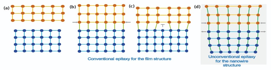
Figure 2. Strain relaxation for crystal materials with lattice mismatch varies between conventional heterostructures and nanowires. (a) Lattices of crystalline materials before epitaxy. (b) Coherent growth by elastic deformation of the epi-layer lattice. (c) Incoherent growth (strain relaxation by mismatch dislocations). (d) Coherent growth by elastic deformation of both lattices. In contrast to the film structure, the lattice in the nanowire structure can deform much more along the radial direction because of its microscale or nanoscale diameter. Thanks to this, nanowires can endure higher strain induced by lattice mismatch.
Researchers have used gold-particle-catalysed vapour-liquid-solid growth to fabricate various nanowires, including those based on GaAs and InP. Using gold is not ideal, because it is incompatible with the mainstream CMOS process and consequently hinders integration of optically active III-V nanowires with silicon technology. Far better alternatives for producing compound semiconductor nanowires by the vapour-liquid-solid growth approach are particle catalysts based on either group III or V elements – and out of these two the former is more suitable.
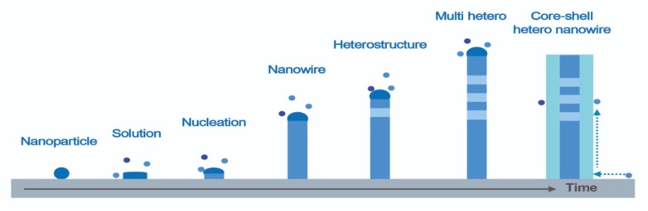
Figure 3. Schematic diagram of the vapour-liquid-solid growth mode. InAs and InP nanowires can be grown by the self-catalysed vapour-liquid-solid mode using indium particles.
The high quality of our structures is evident in high-angle annular dark-field scanning transmission electron microscopy, which reveals the multiple quantum disc layers along the [011] direction (see Figure 4 (c)). Our structures result from a vapour-liquid-solid growth mode that is dominant along the axial direction. Thanks to the low growth temperature, negligible growth occurs in the radial direction via the conventional film growth mode – this is the uncatalyzed mode. With all these factors at play, there is high growth controllability, ensuring homogeneity of the gain medium throughout the entire multiple quantum disc region.
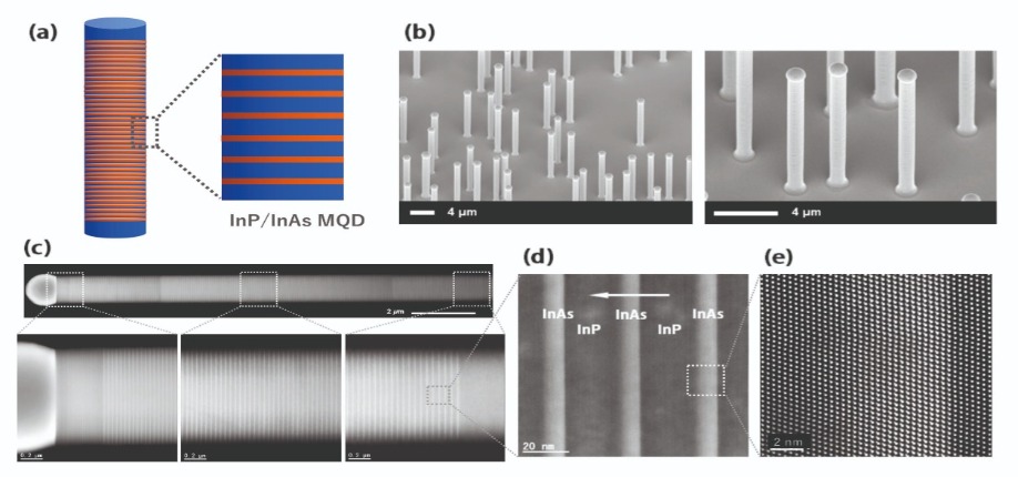
Figure 4. InP/InAs multi-quantum-disc (MQD) nanowires. (a) Schematic diagram of a MQD heterostructure nanowire and a magnified view of the heterostructure highlighting the InP/InAs MQD structure. The InAs layer is indicated in red. (b) Scanning electron microscopy images (tilt: 38º) of InP/InAs MQD nanowires grown on an InP (111)B substrate. (c) High-angle annular dark-field scanning transmission electron microscopy (HAADF-STEM) images of an InP/InAs MQD nanowire taken along the [011] zone axis. The nanowire contains 400 units of InP/InAs heterostructure. ((d) and (e)) Aberration-corrected HAADF-STEM images of InP/InAs heterostructures taken along the [011] zone axis. The horizontal white arrow indicates the growth direction. The thicknesses of the InAs layer and the InP barrier layer are 9.0±1 nm and 25.6±1 nm, respectively.
Creating cavities
We turned to micro-photoluminescence to characterise the optical properties of our nanowires. When they are mechanically dispersed onto foreign substrates, we can remove the indium particles at their tips to create a (111)-facet mirror – and thus a Fabry-Pérot cavity. This structure has intrinsic Fabry-Pérot resonance modes with a sufficiently large mode index in a wide diameter range.
Optically pumping our nanowires leads to lasing behaviour. Measuring the photoluminescence of numerous individual nanowires reveals a broad spontaneous emission spectrum, with a peak wavelength around 1.57 µm to 1.59 µm. When pumped with an excitation power of 2.15 mJ cm-2, a spike centred at 1573 nm appears. Plotting the light input-output curve by varying the excitation power uncovers a strong transition from spontaneous to stimulated emission.
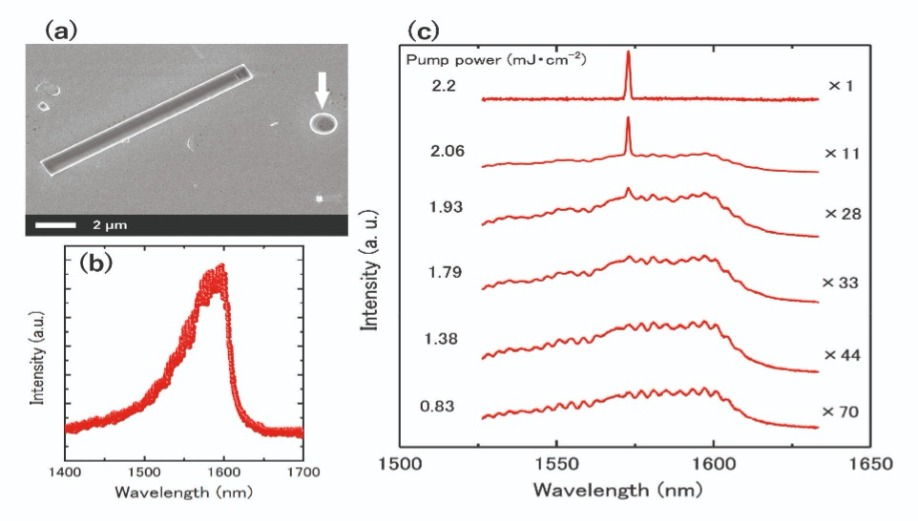
Figure 5. (a) Scanning electron microscopy image of a nanowire mechanically dispersed onto a gold-film-covered SiO2-on-silicon substrate. The white arrow indicates a removed indium particle. (b) Photoluminescence spectrum of a single nanowire under a pump laser power of 0.83 mJ cm-2. (c) Photoluminescence spectra of the nanowire with increasing pump power, revealing spectral narrowing.
So far, we have described optically pumped devices. However, many applications, including photonic integration, demand current-injection light emitters. It is incredibly challenging to realise current-injection lasing from single nanowires, because making a direct electrical contact to them deteriorates light confinement. However, we have taken important steps towards this goal, demonstrating LEDs with p-i-n-structured nanowires that emit in the telecom range.
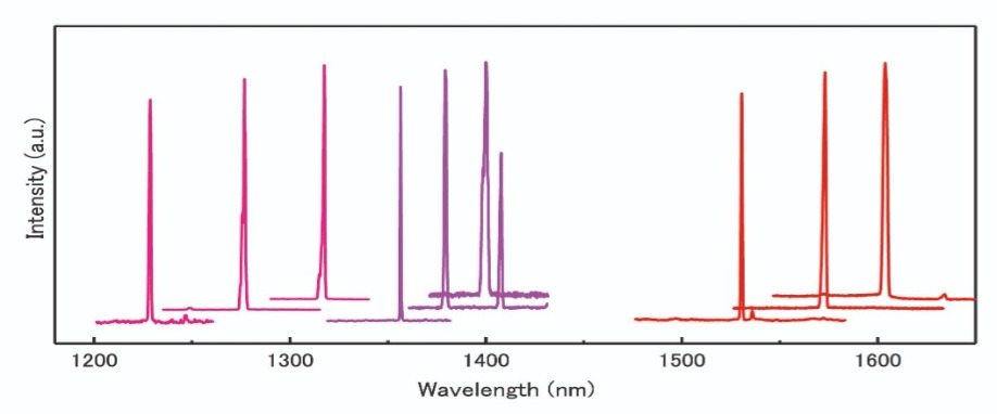
Figure 6. Nanowires allow a tuning of the laser wavelength range in the telecom band. Spectra are offset for clarity. The laser wavelength is modulated by the growth parameters, such as flow rates of the metal-organic sources. Thus a broad wavelength range is covered in the whole telecom band, including the two technologically important telecom-band windows centred around 1.3 µm and 1.55 µm.
To form our novel LEDs, we began by embedding these nanowires in transparent insulating benzocyclobutene. Subsequent reactive-ion etching then removed this organic from the surface, exposed the nanowire tips, and ultimately paved the way to adding electrical contacts. Depositing AuZn metal onto the p-InP substrate and indium-tin-oxide onto the n-InP nanowire segment created electrical contacts for this device.
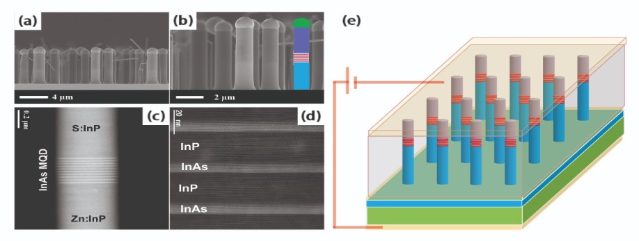
Figure 7. Morphological and structural analysis of InP/InAs heterostructure nanowires. (a) and (b) Cross-sectional scanning electron microscopy images of InP/InAs nanowires. The inset shows the p-i-n structure of these nanowires. (c) and (d), high-angle annular dark-field scanning transmission electron microscopy images of the multi-quantum-disc (MQD) active region between zinc-doped and sulphur-doped InP segments. The MQD active region consisting of 10 InAs quantum discs. (e) A diagram of the nanowire LED device. (Figure reprinted with permission from IOP publishing).
Critical to the development of high-performance optoelectronic devices is tunability of the electroluminescence wavelength. Our multiple quantum disc active region allows us to modulate the photon emission energy by adjusting the thickness of single InAs quantum discs – this alters the quantum confinement along the axial direction. Thanks to the high degree of control provided by vapour-liquid-solid synthesis, we are able to precisely define the thickness of each InAs quantum disc, and thus tune the electroluminescence in the O and E bands of the telecom range.
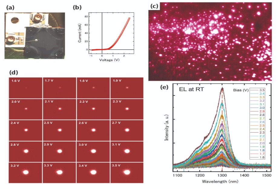
Figure 8. Electrical performance of a nanowire LED at room temperature. (a) The nanowire sample is fixed to a white ceramic substrate with metallic electrodes. The black-colour area is the nanowire LED device (10 µm ×10 µm). (b) A typical current-voltage curve for a nanowire LED. (c) An electroluminescence image taken by an infrared camera under an LED bias of 2.5 V. (d) Electroluminescence images of a single luminescent nanowire with increasing bias (step: 0.1 V). The area of each image is 24 µm × 36 µm. (e) The electroluminescence spectra of the nanowire shown in (d) with increasing bias (step: 0.1 V). The spectra show a constant peak at 1300 ± 5 nm, corresponding to the O-band of telecom-band range. (Figure reprinted with permission from IOP publishing).
G. Zhang et al. ACS Nano 9 10580 (2015)
G. Zhang et al. Nanotechnology 29 155202 (2018)
G. Zhang et al. Sci. Adv. 5 eaat8896 (2019)
H. Sumikura et al. Nano Lett. 19 8059 (2019)
G. Zhang et al. Jpn. J. Appl. Phys 59 105003 (2020)


