
Low voltage GaN designs enable compact 3-phase motor inverter IC
Scientists at Fraunhofer IAF present pioneering integration concepts with GaN-based chips for low-voltage applications
In battery-powered applications, in the automotive sector and in IT infrastructures 48 V technology is on the rise. In this voltage class, GaN power transistors offer the best compromise between safety, compactness and efficiency.
Now, scientists at Fraunhofer IAF have presented pioneering integration concepts with GaN-based integrated circuits for low-voltage applications.
The 48 V class has recently been on the rise and finds application in a wide variety of industries. This is due to the more efficient power transmission it offers compared to lower supply voltages. A change to 48 V is thus a resource-saving alternative for applications that previously used even lower voltages. In contrast to high-voltage power electronics, 48 V offers an ideal compromise between efficiency and safety. There is no need for elaborate safety measures, which renders the voltage class suitable for everyday applications.
Highly integrated GaN components and systems are the ideal solution for 48 V technology. Compared to silicon (Si), GaN has significantly better physical properties for power electronics. In addition, GaN technology allows entire circuit components to be integrated on a chip.
Researchers at Fraunhofer IAF have developed various highly integrated GaN circuits and pioneering integration concepts for low-voltage applications. They presented their research at the leading international conference for power electronics, intelligent drive technology, renewable energies and energy management PCIM 2021.
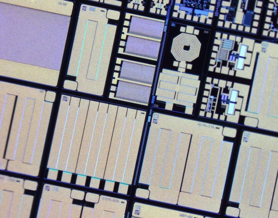
At PCIM, the scientists showed how they merged the two transistors of an integrated half-bridge into a highly compact interleaved design, instead of the usual side-by-side integration, which increases its area-efficiency. They furthermore integrated three such half-bridges into a motor inverter GaN IC for low-voltage applications, and realised an advanced packaging technique for GaN ICs.
Chip layout for low-voltage applications
For several years, GaN-on-Si HEMTs have been an integral component in various power electronics applications, mostly in high voltage systems. At Fraunhofer IAF, it was possible to show how advanced layouts and new analytical design concepts will make GaN devices even more compact and efficient in the future. “In research and development, the focus has so far been mainly on 600 V GaN devices. Concepts for designing highly compact low-voltage GaN power ICs have hardly been explored!” remarks Richard Reiner, a scientist at Fraunhofer IAF, who presented his paper on area-efficient designs for GaN HEMTs at the PCIM 2021.
Advanced packaging for half bridge ICs
“GaN technology allows the integration of a half-bridge consisting of two power transistors in one chip, which significantly increases the compactness of a system. In order to take advantage of this, however, it is extremely important to optimise the integration at the packaging and chip level,” explains Michael Basler, a PhD student at Fraunhofer IAF. The packaging of half-bridge ICs is a challenge due to the high requirements regarding electrical and thermal performance as well as reliability. In his talk at the PCIM, the scientist from Freiburg presented a combination of GaN ICs with PCB embedding technology as an advanced packaging solution that can be extended to a system-in-package and enables extremely high power densities for low-voltage DC/DC converters.
Integrated chip design for motor inverter
In addition to single transistors, commercial GaN low-voltage half-bridge ICs are already available. These half-bridge ICs integrate two power transistors in one chip, but only side-by-side, which does not yet capitalise on the full potential. Fraunhofer IAF has now managed to interleave both half-bridge transistors at the smallest structural level, which further improves efficiency and integrated three of these half-bridge structures into a 3-phase motor inverter GaN IC.
The developer of the motor inverter GaN IC, Stefan Mönch of Fraunhofer IAF, explains the advantages that result from this interleaved structure: “The intrinsic half-bridge improves the electrical switching properties, and all three phases in the same IC reduce the temperature swing during motor operation. Only one IC is also more cost-efficient and easier to build than six transistors or three half-bridges previously needed for a GaN-based motor inverter.”
The presented integration concepts for low-voltage GaN ICs of Fraunhofer IAF show pioneering approaches to material development, packaging designs as well as user-friendly circuits. Such concepts for efficient and compact GaN technologies form a key component for future applications in the 48 V class. The presented technologies have been developed within the research projects GaNTraction (supported by the Vector Stiftung) and GaNonCMOS (funded by Horizon 2020 of the EU).
The publications on the technologies described were published in the anthology of PCIM 2021: ISBN 978-3-8007-5515-8 DNB, Katalog der Deutschen.


