Tackling gallium oxide’s poor conductivity with diamond layers

Growth of diamond layers, realised through high-density seeding of diamond nanoparticles, combats the low thermal conductivity of gallium oxide
For Ga2O3, substantial strengths go hand-in-hand with significant flaws. Thanks to an ultra-wide bandgap, this oxide can withstand very high electric fields, giving it the potential to outperform devices made from SiC and GaN. And unlike those two rivals, Ga2O3, enjoys melt growth of bulk material. However, it is plagued with a lack of p-doping, and a pitiful thermal conductivity of typically just 11-27 W m-1 K-1.
Helping to address the latter issue is a US collaboration that has recently broken new ground by depositing a high thermal conductivity layer, in this case diamond, directly onto a Ga2O3, layer.
Team spokesman, Srabanti Chowdhury from Stanford University, emphasised the importance of this breakthrough by telling Compound Semiconductor that improving heat extraction is crucial for the progress of Ga2O3, power, and RF devices. “However, this thermal management must be cost-effective for both applications, and particularly so for power electronics.”
Cost-constraints hamper the use of large-area single-crystal diamond wafers, which are pricey and limited in size and availability. It is also worth noting that this form of diamond does not give the best results. The thermal boundary resistance for structures constructed by placing small pieces of single-crystal diamond, typically just 3 mm by 3 mm in size, onto Ga2O3, is around 60 m2 K GW-1. A similar figure is found when transferring exfoliated Ga2O3 onto single-crystal diamond, but for the structures produced by the US team, featuring polycrystalline diamond, the thermal boundary resistance is only about 30 m2 K GW-1.
“Our measured diamond-gallium oxide thermal boundary resistance is comparable to those reported for CVD-grown diamond on GaN with about the same silicon nitride dielectric interlayer, which is a very promising result,” enthuses Chowdhury.
The team from Stanford University, The Pennsylvania State University, Georgia Institute of Technology and the University of California, Davies, had to develop a novel process for growing diamond layers. That’s because the direct growth of a diamond layer, by microwave plasma CVD, leads to decomposition of the substrate.
To overcome this issue, the researchers investigated three different approaches to realising high-density seeding: ultrasonication in a nanoparticle solution, drop-seeding, and polymer-assisted seeding.
Ultrasonication seeding failed to realise a continuous layer of diamond. Diamond nanoparticles tended to agglomerate, resulting in a B-Ga2O3 surface unprotected from the plasma. Substrate decomposition followed.
Drop-seeding enabled the deposition of a diamond layer, but it suffered from non-uniformity, due to a very thick seeding layer. And due to differences in thermal expansion coefficient, the diamond delaminated once its thickness exceeded about 200 nm.
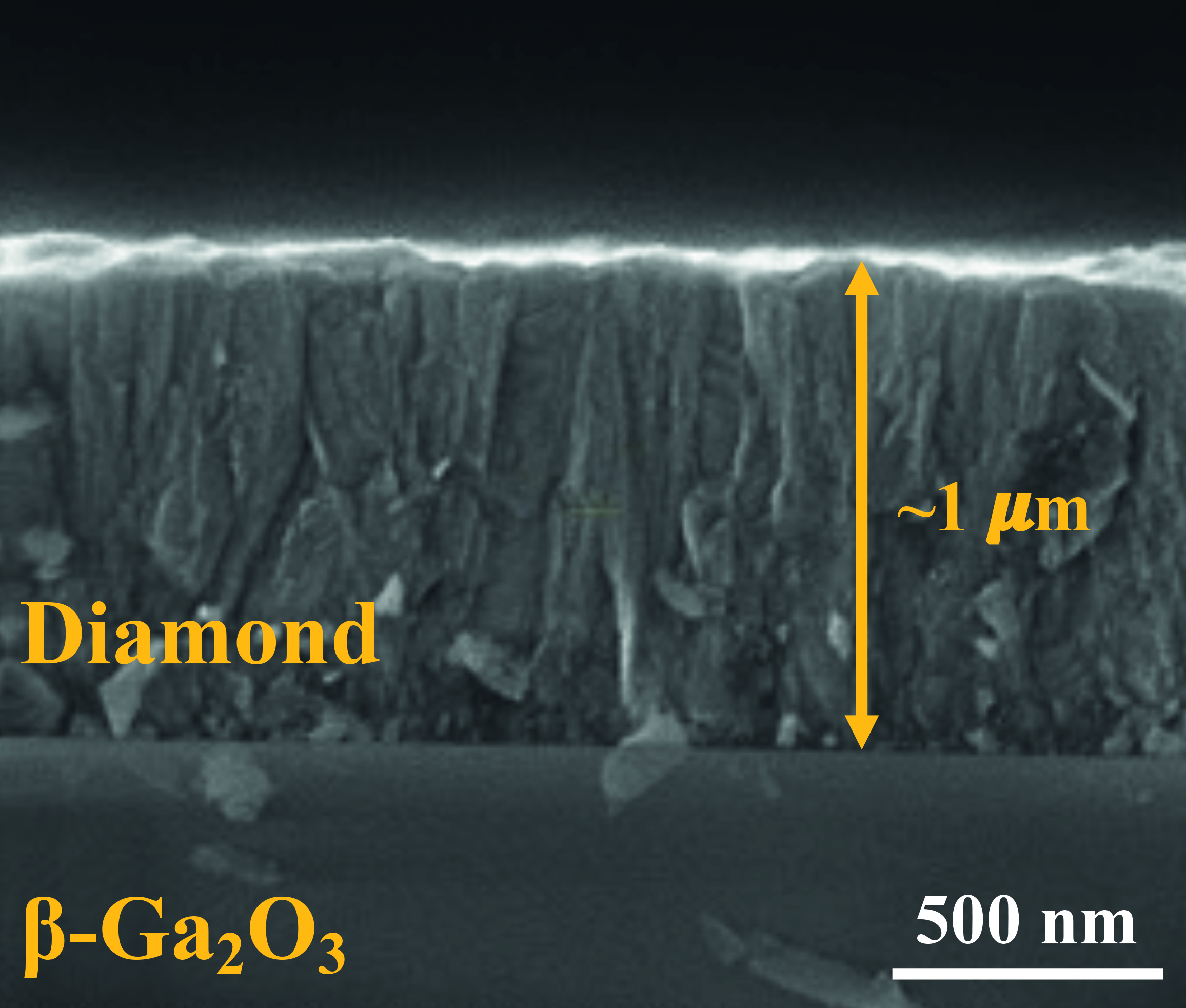
Polymer-assisted seeding produced the best results. The reserachers developed a self-assembly approach, using the polymer to prepare a negative electrostatic surface, before adding nanoparticles with a positive zeta potential. This populated the surface with nanoparticles at a density exceeding 1012cm-2. However, due to the high decomposition rate of B-Ga2O3, in a hydrogen plasma, hydrogen ions threatened to pass through the nanoparticles and inflict damage on the surface of the oxide. To prevent this, the team inserted a thin layer of SiO2 between the B-Ga2O3, and the diamond nanoparticles. This led to the growth of diamond layers.
(The picture above shows growth of a diamond layer on Ga2O3 realised by adding a thin layer of SiO2 and polymer-assisted seeding of diamond nanoparticles.)
Measurements on a sample with a 19 nm-thick layer of SiO2 and a 267 nm-thick layer of diamond revealed a thermal conductivity of 110 W m-1 K-1.
Efforts will now be directed at lowering the thermal boundary resistance and increase the thickness of the polycrystalline diamond, without degrading the properties of Ga2O3.
Reference
M. Malakoutian et al. Appl. Phys. Express 14 055502 (2021)


