
Semiconductor nanoparticles form numerous structures
DESY X-ray study reveals for the first time how lead sulphide particles self-organise in real time
The structure adopted by lead sulphide semiconductor nanoparticles changes surprisingly often as they assemble to form ordered superlattices. This is revealed by an experimental study at PETRA III, the storage-ring-based X-ray radiation source run by DESY (Deutsches Elektronen-synchrotron) the largest centre for high-energy particle-physics research in Germany.
The results have been published in the journal Chemistry of Materials. The study helps to better understand the self-assembly of nanoparticles, which can lead to significantly different structures.
Among other things, lead sulphide nanoparticles are used in photovoltaic cells, LEDs and other electronic devices. In the study, a team led by DESY scientists Irina Lokteva and Felix Lehmkühler, from the Coherent X-ray Scattering group headed by Gerhard Grübel, has observed the self-organisation of these semiconductor nanoparticles in real time.
They did so by placing a drop of liquid (25 millionths of a litre) containing the nanoparticles inside a small cell and allowing the solvent to evaporate slowly over the course of two hours. The scientists then used an X-ray beam at the P10 beamline to observe in real time what structure the particles formed during the assembly.
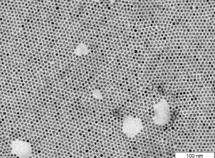
To their surprise, the structure adopted by the particles changed several times during the process. “First we see the nanoparticles forming a hexagonal symmetry, which leads to a nanoparticle solid having a hexagonal lattice structure,” Lokteva reports. (The picture at the top of the page above shows how lead sulphide nanoparticles, which are about 8nm in size, initially arrange themselves into a layer with hexagonal symmetry.)
“But then the superlattice suddenly changes, and displays a cubic symmetry. As it continues to dry, the structure makes two more transitions, becoming a superlattice with tetragonal symmetry and finally one with a different cubic symmetry.” This sequence has been never revealed before in such detail.

The team suggests that the hexagonal structure (hexagonal close-packed, HCP) persists for as long as the surface of the particles is swollen by the solvent. Once the film dries a little bit, its internal structure changes to a cubic symmetry (body-centred cubic, BCC). However, residues of the solvent still remain between the individual nanoparticles inside the film. As this evaporates, the structure changes two more times (body-centred tetragonal BCT and face-centred cubic FCC).
The final structure of the film depends on a number of different factors, as Lokteva explains. They include the type of solvent and how quickly it evaporates, size and concentration of the nanoparticles, but also the nature of the so-called ligands that surround the particles and their density. Scientists use the term ligand to describe certain molecules that bind to the nanoparticle surface and prevent them from agglomeration. In the study, the team used oleic acid for this purpose; its molecules cover the particles, much like the wax that prevents gummy bears from sticking to each other in a bag. This is a well-established process in nanotechnology.
“Our research indicates that the final structure of the superlattice also depends on whether the individual nanoparticles are surrounded by many or few oleic acid molecules,” reports Lokteva.
“In an earlier study, we obtained films with a BCC/BCT crystal structure when the ligand density was high. Here, we specifically looked at nanoparticles with a low ligand density, and this led to an FCC structure. So when using nanoparticles, the ligand density ought to be determined, which is not a standard practice at the moment,” explains the DESY scientist.
'Real-Time X-ray Scattering Discovers Rich Phase Behavior in PbS Nanocrystal Superlattices during In Situ Assembly' by Irina Lokteva et al; Chemistry of Materials, 2021


