Pushing the power envelope

Novel designs enrich the performance of power devices employing a range of semiconducting materials.
BY RICHARD STEVENSON, EDITOR, CS MAGAZINE
LONG GONE are the days when the likes of GaN and SiC were just promising materials. Now they are fulfilling their potential, evidenced by their significant commercial success. Sales of SiC MOSFETs are soaring, thanks to their widespread deployment in electric vehicles, and GaN is now established as the material for making fast chargers for portable devices.
But the revolution in power electronics is by no means over. For operation at a few kilovolts of more, the leading devices are still the silicon IGBT and thyristor. However, looking to replace them are a number of novel alternatives – they may also have a role to play at lower voltages – that are based on compound semiconductor materials.
Several strong examples of these devices featured at the latest IEEE International Electron Devices Meeting (IEDM), held in San Francisco, California, from 9-13 December. Many advances were discussed at that meeting, including: the first demonstration of a trench-shaped 6.5 kV SiC IGBT; GaN HEMTs capable of blocking that voltage while delivering an ultralow dynamic on-resistance; the first vertical superjunction device made from Ga2O3, offering a breakdown voltage of 2 kV; and AlN-based vertical p-n diodes with dopant-free distributed-polarisation doping that feature a critical electric field almost twice that of reported values for SiC and GaN.

Figure 1. The n-channel SiC IGBT with a trench-etched double-diffused MOS structure.
Trench-shaped SiC IGBTs
Efforts at the national level to trim carbon footprints need to include the introduction of smart grids and high-voltage direct-current transmission systems. For both these innovations, the building blocks include static synchronous compensators and solid-state transformers, components that are formed from power devices capable of blocking high voltages and delivering high currents.
Devices made from SiC are promising candidates for serving in these compensators and transformers. As well as ensuring a high performance at the device level, the capability of SiC to operate at high frequencies opens the door to trimming the size and increasing the efficiency of the compensators and transformers. However, if 6.5 kV SiC MOSFETs are deployed, the on-resistance is a concern, particular at elevated temperatures – at 175 °C, it’s 104 mΩ cm2.
Due to this limitation, a number of research groups have already developed SiC IGBTs. They include those capable of blocking 15 kV by utilising a thick drift layer, and variants pioneered by Hitachi that feature a thinner drift layer to trim switching loss. In 2016 researchers from Hitachi unveiled a 6.5 kV SiC IGBT with a low switching loss that employed an extremely thin drift layer, and at the latest IEDM this team introduced a descendent with a trench-etched double-diffused MOS structure (see Figure 1), designed to address low electron injection from the emitter, due to poor channel mobility.
Describing this device in his IEDM presentation, Naoki Watanabe emphasised a weakness in more conventional SiC trench-gate structures: “At the trench bottom, high electric fields occur in the gate oxide in the off state, due to the high critical electric field of silicon carbide, which is close to the gate oxide. Therefore, electric field relaxation is necessary to realise trench-gate silicon carbide IGBTs.”
Addressing this issue is the team’s novel form of SiC IGBT, which features a trench-etched double-diffused MOS structure. It is claimed that one of the merits of this design, which utilises a V-shaped structure, is an increased channel density, realised by shrinking the trench pitch. Another strength is that during operation in the off-state, the electric field in the gate oxide is greatly decreased, by burying the trenches in the p-body.
To evaluate the capability of the trench-etched double-diffused MOS structure, Watanabe and co-workers produced a test structure of that form, before comparing its electrical characteristics to that of a planar variant. Plotting the gate voltage as a function of drain current revealed a doubling of the current with the trench-etched double-diffused MOS structure, attributed to the fin shape. “Therefore, the electron injection from the emitter can be enhanced by the trench-etched double-diffused MOS structure,” argued Watanabe.

Figure 2. A blocking voltage of more than 6.5 kV is realised with the
SiC IGBT with a trench-etched double-diffused MOS structure.
Simulations by the team offered an insight into the electric fields within the device in the off-state, thought to peak at 2 MV cm-1. “This is low enough to ensure a high reliability,” claimed Watanabe, who added that the trench-etched double-diffused MOS structure suppresses the electric field in the gate oxide.
Fabrication of the team’s novel IGBTs began by taking an n+ substrate and depositing an epistructure that included a 70 µm-thick drift layer. By using backside grinding as the last process, IGBTs were produced with a thin drift layer.
Measurements of electrical characteristics revealed that the on-voltage, defined as the voltage for a collector current of 200 A cm-2, is 4.8 V for the IGBT with the trench-etched double-diffused MOS structure, compared with 6.7 V for the planar control. At turn-on, the novel IGBT had a differential on-resistance of 6.6 mΩ cm2, roughly a third of that of the planar device. The blocking capability of the IGBT with the trench-etched double-diffused MOS structure is demonstrated by the collector leakage current of 0.41 mA cm-2 at 6.5 kV (see Figure 2).
The switching characteristics of the IGBT with the trench-etched double-diffused MOS structure are also superior to the planar control. Losses for turn-off and turn-on are around 19 percent and 6 percent lower, thanks to a small feedback capacitance and a large electron injection from the emitter.
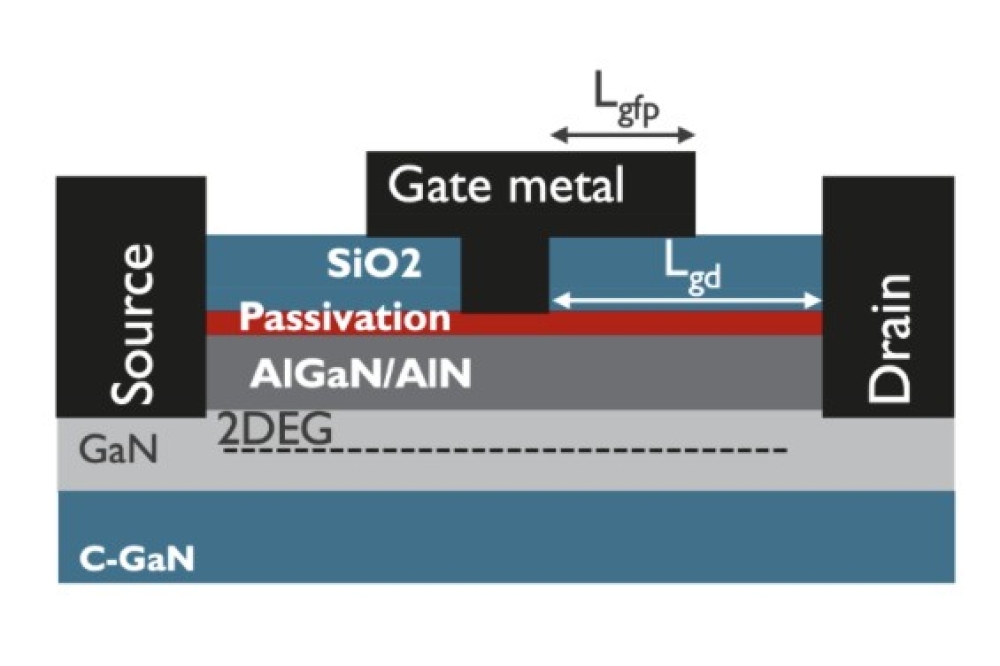
Active passivation GaN HEMTs
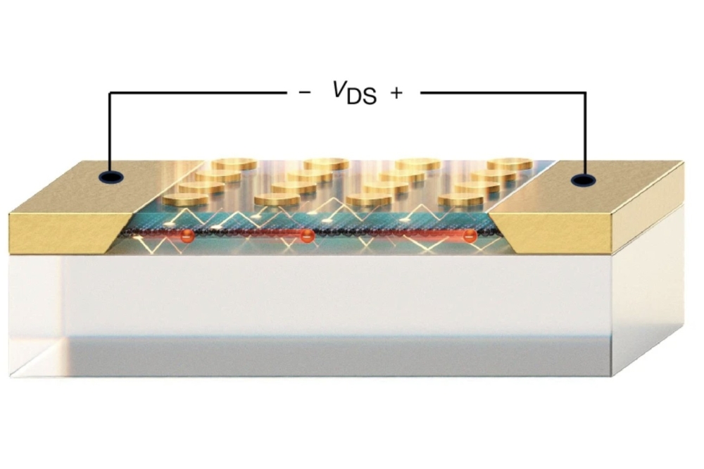
Another device showcased at IEDM that’s capable of delivering a 6.5 kV blocking voltages and is targeting tomorrow’s electrical grid infrastructure is the E-mode active-passivation p-GaN gate HEMT. Developed by a partnership between researchers at Peking University, Tsinghua University and Nagoya University, this form of lateral GaN HEMT, which is grown on a sapphire substrate, has merits that include avoiding the need for a thick epitaxial structure and the opportunity to use the same epiwafer for low-voltage and high-voltage devices.
Speaking on behalf of the team, Jiawei Cui from Peking University remarked that two of the challenges faced when developing kilovolt-level GaN power switches are ensuring enhancement-mode operation – that is, the devices are normally off – and the stability of the dynamic on-resistance.
“The p-GaN gate HEMT is a mainstream technology for E-mode GaN power transistors,” said Cui. “To make full use of the experiences accumulated in the past years, we think it’s a good choice to use the p-GaN gate structure for high-voltage transistors as well.”
To suppress dynamic on-resistance, Cui and co-workers have moved away from the traditional methodology of adding multiple field plates, an approach described as impractical for devices operating at several kilovolts of more.
“As an alternative, we propose the active-passivation p-GaN gate HEMT,” remarked Cui, who explained that a thinned p-GaN layer provides passivation in this transistor (see Figure 3). Additional features of this form of HEMT are the screening of surface trapping by mobile holes, and the use of just a single additional step to provide active passivation.
Fabrication of the team’s devices began by taking a conventional epiwafer featuring a high-resistivity buffer layer, a 200 nm-thick undoped GaN channel, a 15 nm-thick Al0.2Ga0.8N barrier and a 20 nm-thick p-GaN cap, and selectively etching into this layer with a two-step process. SiO2 deposition to passivate the device followed, prior to the addition of ohmic contacts, an isolation step, and the formation of a gate contact and probe pad.
Electrical measurements revealed that the active-passivation HEMT has a superior off-state blocking capability than the conventional HEMT, which acts as a control. For both devices, increases in gate length led to a higher blocking voltage, with the activate-passivation HEMT with a 77 µm-long gate capable of blocking 6.573 kV (see Figure 4). The team attributed the higher blocking voltage for the active-passivation HEMT to a shift in the location of the depletion region, so that it no longer sits partially below the gate.

Figure 3. The architecture of the active-passivation HEMT (a) and an outline of its fabrication process (b).
According to measurements of transfer current-voltage characteristics, both forms of HEMT exhibit enhancement-mode operation, with a threshold voltage of 0.8 V.
Measurements of the output current-voltage characteristics revealed that the on-resistance for the HEMT with active passivation is lower that than for the control – the values were 38.2 mW mm and 43.6 mW mm, respectively.
To evaluate the dynamic on-resistance of their devices, Cui and co-workers compared dynamic and static values at a range of drain-source voltages. The ratio is low, with 1.02 reported for measurements at 4.5 kV on enhancement-mode p-GaN gate HEMTs with a 77 µm gate length.
The excellent on-resistance characteristics are claimed to result from the screening effect, due to the passivation layer. To validate this attribution, the team produced a pair of devices – with and without active passivation – that included a surface testing electrode.
Applying a negative voltage to this electrode mimicked the negative surface trapping effect. “It is found that the drain current in the conventional HEMT reduces, but the drain current in the active-passivation HEMT remains unchanged,” said Cui. “The result suggests that active passivation can screen the surface effect from influencing the 2DEG channel.”
The researchers also carried out a second test, applying a positive voltage to the electrode to trap electrons at the surface. When this voltage is removed, the drain current in the conventional HEMT reduced, and took a long time to recover. In comparison, the active-passivation HEMT did not produce a change in drain current, providing further evidence of surface screening.
Cui concluded his talk by benchmarking the active-passivation HEMT. He claimed that this device, delivering a performance close to the SiC limit, is the first enhancement-mode p-GaN gate HEMT with a blocking voltage of 6.5 kV or more.
Ga2O3 superjunction Schottky rectifiers
Another claim of breaking new ground came from a collaboration between researchers in the US and Japan: the first vertical superjunction device made from the ultra-wide bandgap material Ga2O3.
This partnership between researchers at Virginia Polytechnic Institute and State University, the University of Southern California, the US Naval Research Laboratory, Novel Crystal Technology, and Oak Ridge National Laboratory, produced a portfolio of devices featuring pillars 1-2 µm wide, wrapped in charge-balanced p-type NiO. These devices can block up to 2 kV.
Speaking on behalf of the partnership, Yuan Qin from Virginia Polytechnic Institute and State University, began his presentation by emphasising the strengths of Ga2O3. They include a high critical electric field – it is projected to be up to 8 MV cm-1 – a high temperature stability, and the possibility for epitaxial growth on large-diameter substrates. Unfortunately, this oxide has two major downsides: a lack of p-type doping and a low thermal conductivity.
Qin offered a brief overview of the evolution of all forms of semiconductor device, explaining that the switch from one-dimensional structures to multi-dimensional variants, such as those employing a superjunction, multiple channels and multiple gates, has enabled a higher power density and efficiency at the system level.

Figure 4. The off-state characteristics of the conventional GaN HEMT (a)
are inferior to the variant with the active-passivation design (b)
For superjunction devices, such as those made by Qin and co-workers, there is a linear increase in on-resistance with blocking voltage, while for one-dimensional variants, the on-resistance scales with the square of the blocking voltage.
“For the ultra-wide bandgap semiconductor gallium oxide there are still some challenges for fabricating superjunction devices,” remarked Qin, who explained that one of them is the development of a deep pillar etch process that produces a vertical sidewall and smooth surfaces.
Due to the lack of p-type Ga2O3, device development also requires the selection of an alternative p-type material that does not lead to excessive interface traps. NiO is an obvious candidate – it has previously been used for fabrication of vertical superjunctions in GaN and lateral superjunctions in Ga2O3.
Fabrication of the superjunction devices involved processing a 2-inch Ga2O3 epiwafer produced by NCT that has a 10 µm-thick layer of n-Ga2O3 with a doping level of 2 x 1017 cm-3, and a 0.5 µm-thick layer of n-Ga2O3 with a doping level of 1 x 1016 cm-3. Dry etching produced 6.5 µm-deep pillars, wrapped in NiO by conformal sputtering in an atmosphere of argon and oxygen. As the acceptor concentration in the NiO is much higher than the donor concentration in the Ga2O3 pillars, NiO with a thickness of 120 nm provides charge balancing with 1-2 µm-wide pillars. The team completed the fabrication of their devices by filling the trenches with a photoresist and adding a Ni/Au/Ti/Ag Schottky contact (see Figure 5 for the device architecture, and Figure 6 for more details of the process flow).

Figure 5. Characteristics of the vertical Ga2O3 superjunction Schottky
barrier diode are determined by key dimensions, such as the trench depth
(LSJ), the trench depth (Wn), the separation distance between the
trenches (S), and the thickness of the NiO (Wp).
With this design, the 0.5 µm-thick top n-Ga2O3 layer serves two purposes: it lowers the tunnelling leakage current of the Schottky contact; and it shifts the position of the peak electric field from the Schottky contact to the bulk superjunction.
Qin and co-workers evaluated the blocking capability of superjunction devices with a range of pillar widths. They found that the breakdown voltage initially increased with pillar width, reaching 2 kV at a width of 1.8 µm, before declining at wider widths. The peak blocking capability results from optimal charge balancing.
As the device temperature increased to 175 °C, the team observed a small reduction in blocking voltage to 1.8 kV. This suggests that the charge balance is preserved at high temperatures.

Figure 6. The ten-step process to produce Ga2O3 superjunction Schottky barrier diodes.
For the device with the best blocking voltage, at room-temperature turn-on occurred at 1 V, the on-off ratio was around 109, and the specific on-resistance just 0.7 mΩ cm2. At 175 °C, the turn-on voltage fell to 0.8 V, the on-off ratio was around 108, and the specific on-resistance 1.3 mΩ cm2.
Benchmarking this device, Qin remarked that it offers the best trade-off between the specific on-resistance and the breakdown voltage for all Schottky barrier diodes and junction barrier Schottky diodes from 600 V to 4 kV. The performance of the team’s device, which offers fast switching, is close to the one-dimensional limit for GaN.

Figure 7. Distributed polarisation doping is used to form the AlN-based diode.
AlN vertical p-n diodes
Of all the alternatives to silicon, AlN arguably has the greatest promise. Thanks to a bandgap of 6 eV, it has a much higher critical electric field than all its rivals, indicating the potential for an improved trade-off between the blocking voltage and the specific on-resistance.
For many years, one of the drawbacks of AlN devices has been the lack of native substrates. However, much progress has been made in recent years, with reports from 2022 revealing that threading dislocation densities in this material can be below 104 cm-2, and Asahi Kasei announcing 4-inch diameter substrates in 2023.
Another issue with AlN is the difficulty in realising conductive layers. Due to high ionisation energies for the common dopants – for the silicon donor it is 282 meV, and for the magnesium acceptor it is 630 meV – room temperature conductivity via conventional approaches is a challenge.
Offering a solution is distributed polarisation doping, and approach pioneered at the University of California, Santa Barbara, just over 20 years ago. Both p-type and n-type conductivity can be realised in nitride alloys by using positive or negative fixed space charges that depend on the graded direction.
Building on this approach, a team from Nagoya University and Asahi Kasei has used distributed polarisation doping to produce a p-type layer in AlN-based laser diodes. This approach to producing a p-type layer is said to increase the injection efficiency and trim series resistance, and ultimately enable the demonstration of a laser with continuous-wave emission in the UVC.
At IEDM that team announced further success with distributed polarisation doping, using this to produce both p-type and n-type layers in an AlN-based vertical p-n diode.
Speaking to the IEDM delegates, Takeru Kumabe from Nagoya University explained that until their team’s recent success, AlGaN diodes with an aluminium composition exceeding 30 percent that exhibited ideal electrical characteristics had not been realised.
Kumabe and co-workers produced their devices by taking an AlN substrate and growing a 300 nm-thick Al0.7Ga0.3N contact layer, followed by a 400 nm AlGaN n-type layer with distributed polarisation doping, a 120 nm-thick p-type layer with distributed polarisation doping, and finally a 20 nm-thick magnesium-doped GaN contact. In the layers with distributed polarisation doping, aluminium content in the AlGaN layers ranged from 70 percent to 95 percent.

Figure 8. The temperature-dependent ideality factor of the AlN diode is
close to 2, indicating that electrons and holes both play a role in
device operation.
Fabrication of the diodes began by activation of magnesium dopants in the capping layer. Etching defined the vertical mesa and plasma-enhanced CVD provided a protecting layer of SiO2, prior to addition of the cathode, anode and contact pad, and a polyimide surface protection layer to prevent air discharge.
Secondary ion mass spectrometry (SIMS) determined average values for the negative and positive charge concentrations of 1.8 x 1018 cm-3 and 2.6 x 1017 cm-3, respectively. “In both distributed polarisation-doped layers, charge concentration was constant along the depth direction, thanks to the linear compositional grading,” explained Kumabe, who added that the results from SIMS and X-ray reciprocal spacing mapping indicate that the structure fulfils its intended design.
Electrical measurements at room-temperature on the diodes revealed a turn-on voltage of 6.5 V and a specific on-resistance of 3 mΩ cm2. According to Kumabe, this is the smallest value for specific on-resistance ever reported for AlN-based p-n diodes.
The team have also used electroluminescence (EL) to scrutinise the behaviour of their devices. “The EL emission increased with increasing current, suggesting that both electrons and holes contributed to the conduction of typical p-n diodes,” remarked Kumabe.
To verify that their device is a true p-n diode, Kumabe and co-workers measured the current density as a function of forward bias at temperatures from 323K to 573K, finding that threshold voltage decreased with increasing temperature. Using the recombination current model to describe the electrical behaviour provided further evidence that the team’s device behaves as a p-n diode, rather than one with a metal-insulator-semiconductor structure (see Figure 8).
Reverse-bias measurements revealed a destructive device breakdown at -283 V, indicating avalanche breakdown did not occur. This led Kumabe and co-workers to calculate an electric field at breakdown of 7.3 MV cm-1.

Figure 9. The performance of the AlN-based diode with distributed polarisation doping is well beyond the SiC and GaN limit.
“The extracted electric field was compared with silicon carbide and gallium nitride electric field limits, as well as previously reported distributed-polarisation-doped GaN p-n diodes,” said Kumabe. “The value of 7.3 MV cm-1 was almost twice as high as the gallium nitride and silicon carbide limit with the same doping concentrations.”
Kumabe also noted that their device broke the limit of what could be realised by distributed-polarisation-doped GaN diodes on GaN substrates.
“This result demonstrates the high potential of aluminium nitride and high-aluminium content aluminium gallium nitride in power device applications,” concluded Kumabe.
Such work shows that great progress is being made with AlN devices. Alongside advances in SiC, GaN and Ga2O3 devices, reported at IEDM and elsewhere, there’s no doubt that the revolution in power electronics is well underway – but more is still to come.