Accelerating the AlGaN HEMT
HEMTs with a Al0.25Ga0.75N channel combine record-breaking speeds with an impressive breakdown voltage
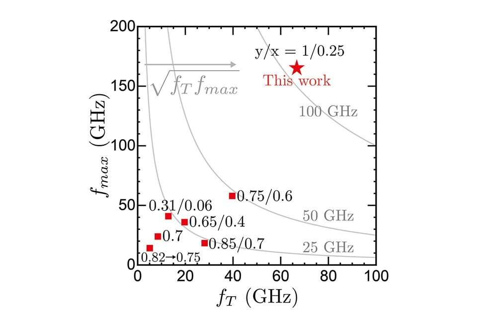
Researchers from Cornell University are claiming to have broken the speed record for AlGaN-based transistors. The team’s HEMTs, which have a T-shaped gate and an Al0.25Ga0.75N channel, have a cut-off frequency, fT, of 67 GHz, and a maximum oscillation frequency, fmax, of 166 GHz.
Another asset of these transistors is an average breakdown field exceeding 2 MV cm-1. This helps to ensure a high value for Johnson’s figure of merit – the product of the breakdown voltage and fT – and highlights the potential of these device for serving in next-generation high-power RF applications.
Replacing the GaN channel of a HEMT with an AlGaN alloy has much promise, as it has the potential to increase the breakdown voltage due to the higher bandgap, while having no impact on the saturation velocity, so should not impede the speed of the transistor. However, success is not easy – increases in aluminium content in the channel make it harder to realise ohmic contacts, and there is the possibility that the additional aluminium content leads to low-field mobilities, resulting in a higher sheet resistance and parasitic delay, hampering the speed of the device.
To overcome these difficulties, the team applied re-grown ohmic contacts that cover the sidewall of the channel, which had a carefully selected composition to maximise fT, fmax, and the breakdown voltage.
The record-breaking devices produced by the team do not contain a field plate, creating a design with the potential to provide cost savings in high-voltage RF applications.
According to one of the researchers speaking on behalf of the team, Eungkyun Kim, the addition of a field plate would increase the breakdown voltage, reduce the effect of RF dispersion by spreading out the peak electric field near the drain-side gate edge, and ultimately enable a higher output power density in the X-band. “However, due to the extra parasitic capacitance induced by the field plate, power amplification at higher frequencies might become challenging.”
Fabrication of the team’s HEMTs began by loading a semi-insulating 6H-SiC substrate into a plasma-assisted MBE chamber and depositing a 1 mm-thick AlN layer, followed by a 24 nm-thick Al0.25Ga0.75N channel and a 15 nm-thick AlN buffer layer. Electron-beam lithography defined a T-shaped Ni/Au gate, prior to the addition of a SiN passivation layer that ensures improved dispersion control.
Measurements on devices with a 70 nm gate length and a source-to-drain width of 600 nm revealed a contact resistance for the n+ GaN non-alloyed ohmic contacts of 0.23 W mm, which is claimed to be amongst the lowest values for contact to the two-dimensional electron gas in AlGaN-channel HEMTs.
The value for the DC output conductance exceeds that of previous reports, suggesting the presence of short-channels effects, which could be suppressed by thinning the top AlN barrier.
Biasing at a gate-source voltage of -4 V and a drain-source voltage of 10 V produced a peak transconductance of 0.1 S mm-1. These bias conditions were also used to obtain values for fT and fmax.
For a gate-to-drain distance of 260 nm, the HEMT produced a breakdown voltage of 59 V, equating to an average breakdown field of more than 2 MV cm-1.
Benchmarking their devices revealed that the average geometric mean of fT and fmax, which is 105 GHz, is significantly higher than all previous reported results (see figure above. The numbers beside the data points refer to the aluminium content in the top barrier and channel layer, respectively.).
The team are now considering a switch to nitrogen-polar heterostructures to improve ohmic contacts to their AlGaN-channel HEMTs. This modification would remove the electrically insulating AlN layer on top of the channel, and open up the possibility to make an ohmic contact to AlGaN.
Reference
E. Kim et al. Appl. Phys. Express. 16 111003 (2023)