Cutting the cost of InP-based devices

Engineered InP-on-GaAs substrates with diameters up to 200 mm provide a rigid, low-cost platform that can be rapidly ramped to production volumes.
BY FRANK DIMROTH, CARMINE PELLEGRINO, JENS OHLMANN AND DAVID LACKNER FROM FRAUNHOFER ISE AND JÖRG SCHWAR FROM III/V-RECLAIM
Our industry is driven by constant demand for materials offering superior performance, scalability, and cost-effectiveness. Devices utilising III-V compounds on InP boast unique properties, such as the exceptionally high electron mobility of InGaAs and the ability to absorb and emit infrared light up to 1500 nm and beyond. Thanks to these features, devices based on InP and its related alloys are ideal for a number of high-end applications, including infrared cameras, photodetectors, and high-speed transistors. However, although InP substrates have been the gold standard for such applications, their high cost and limited availability pose significant challenges for large-scale production.
To address these concerns, our collaboration between Fraunhofer ISE and III/V Reclaim has been developing an innovative technology that leverages our expertise in growing metamorphic materials as well as polishing them to create high-quality InP layers on GaAs substrates. Our progress has led us to release a new product, the InP-on-GaAs engineered substrate, that can effectively replace a standard InP wafer in a wide variety of applications. This novel substrate, now available in 4-inch and 6-inch diameters, with the opportunity to scale to 8-inch on the horizon, delivers comparable performance to pure InP while significantly reducing costs and enabling higher production volumes. Due to these strengths, our new substrates are the ideal choice for manufacturers looking for competitiveness in a rapidly evolving market.
Figure 1. (a) An illustration of the InP-on-GaAs engineered substrate, including a GaAs substrate, an engineered stack of epitaxial buffer layers and the final relaxed InP surface layer. An atomic force microscope image shows the surface morphology and (b) a cathodoluminescence image reveals the low threading dislocation density (TDD) of 1-5 x 106 cm-2. (c) A white-light interferometric microscopy image reveals a surface roughness, Ra, of 0.1 nm, comparable to prime InP wafers.
InP bulk substrates present significant challenges for large-scale production of optoelectronic devices. Among a number of concerns, the most significant are probably a high cost, brittleness, and limited availability. These weaknesses can be attributed to the process used for manufacturing high-quality InP ingots for wafer fabrication – compared to that employed for producing GaAs, it is more complex and necessitates more costly equipment. The complexity arises from the intrinsic properties of InP, such as its high decomposition pressure at its melting temperature and its greater tendency to twin. Due to these factors, stricter quality assurance standards are essential for managing defects and ensuring wafer quality.
Another downside of the high complexity of the InP production process is that it hampers scalability, limiting availability of larger substrate sizes.
Currently, InP substrates are predominantly available in sizes ranging from 2-inch to 4-inch, with the 6-inch variant only recently entering production. This limited range of diameters is a key obstacle to upscaling. Efforts on magnifying dimensions are also impaired by the brittleness of InP that increases the risk of breakage during device fabrication, and leads to a lowering of production yield that escalates costs.
On top of that, InP technologies rely on indium, a relatively rare and expensive element. Market prices for this metal can be volatile, due to a limited supply, as well as high demand in various industries. For instance, last year indium prices shot up by 50 percent. This factor, alongside others just outlined, collectively hinder the widespread adoption and economical mass production of InP-based optoelectronic devices.
Figure 2. (a) Sketch of the laser power converter grown on InP and InP-on-GaAs substrates. (b) Calibrated internal quantum efficiency (IQE) of laser power converters grown on a reference InP substrate (orange diamonds) and on an InP-on-GaAs engineered substrate (green circles). (c) Open circuit voltage (VOC) measured at a photocurrent density (JSC) of 25 mA cm-2 for the laser power converter grown on InP (orange line) and for different generations of InP-on-GaAs substrates (green symbols). Our latest generation of InP-on-GaAs substrates (Gen-2) feature VOC values only 15 mV below the reference device on a InP bulk substrate.
In comparison, the GaAs industry holds significant advantages in terms of large-scale production, since GaAs substrates are generally less expensive to produce, thanks to more mature manufacturing processes refined over many decades. Unlike InP, GaAs substrates are more robust and available in formats up to 8-inch diameter, making them better suited to high-volume manufacturing. The higher stability of GaAs also allows for thinner wafers, consuming fewer of the precious metals. These factors make GaAs a more cost-effective and practical choice for large-scale production of optoelectronic devices.
Integrating InP-based technologies onto GaAs substrates is far from easy, due to one of the most critical challenges in semiconductor manufacturing: the lattice mismatch. There is a difference in atomic spacing of almost 4 percent between InP and GaAs, hindering high-quality epitaxial growth of InP directly on GaAs due to defects forming uncontrolled throughout the layer structure. Harmful defects, also known as threading dislocations, act as recombination centres that slash carrier lifetimes, leading to severe degradation in device performance and efficiency.
By capitalising on our long-standing expertise in developing metamorphic materials, we have developed a robust manufacturing process that ensures that our InP-on-GaAs substrates are of the highest quality. Our final InP-on-GaAs wafer (see Figure 1 (a)) features a GaAs substrate, topped with a series of epitaxial buffer layers, culminating in an almost fully relaxed InP surface. This surface, with a threading dislocation density in the range of just 1-5 x 106 cm-2 “(see Figure 1 (b)), serves as a virtual substrate for subsequent epitaxial growth of InP-based devices. Thanks to this excellent material quality, our engineered wafers ensure reliable performance, even for devices sensitive to degradation in carrier lifetime.
Figure 3. (a) Open-circuit voltage (VOC) map of a 6-inch InP-on-GaAs substrate populated with InGaAs laser power converters. Each pixel with coordinate (x,y) corresponds to an individual device with a nominal area of 5.4 mm2. A total of 826 cells were processed and measured. The photocurrent density was on average 7.98 A cm-2 with a standard deviation of 0.11 A cm-2. The VOC performances are reported in histograms in (b).
To ensure an epi-ready surface, our as-grown wafers undergo a specialised chemical mechanical polishing process. According to white-light interferometric microscopy, these engineered substrates have exceptional surface morphology, with an arithmetic mean roughness (Ra) of just 0.1 nm, a figure that’s comparable to prime InP wafers.
One of our latest experiments provides a representative example of what can be expected with our novel wafers. To provide a fair comparison of the performance of devices made on InP and on InP-on-GaAs, we have fabricated an In0.53Ga0.47As laser power converter (band gap of 0.74 eV) on both a 4-inch pure InP wafer and a 6-inch InP-on-GaAs engineered substrate (the device structure is outlined in Figure 2 (a)). By employing identical epitaxial growth and processing steps, we effectively produced the same device on both substrates.
We have compared the performance of these devices using electro-optical characterisation. Calibrated internal quantum efficiency measurements produce very similar values for photocurrent generation efficiency for devices on InP-on-GaAs and reference InP substrates (see Figure 2 (b)). For the performance metric of the p-n junction, we considered the open-circuit voltage of our power converters, measured at a photocurrent density of 25 mA cm-2. The two types of device produced similar values for this metric, with that grown on InP delivering an open-circuit voltage that’s higher by 15 meV. Our view is that there is the potential to close even this small gap by fine-tuning the growth conditions, a step that we did not take in this investigation.
While a high-performance is encouraging, manufacturers need good results for all devices across a wafer. The good news is that our engineered substrates fulfil this crucial citeria, with exceptional performance consistency realised across the entire 6-inch substrate area. This strength ensures high productivity by maximising the usable wafer area.
To highlight the great degree of uniformity of devices produced with our technology, we have produced a dense matrix of pixel cells, each with a nominal active areas of 5.4 mm². Fabrication involved mesa-etching of every pixel to ensure electrical isolation from adjacent cells. This step has enabled accurate on-wafer characterisation.
In total, we have processed 826 devices on one half of a 6-inch wafer, using a pixel pitch of 2.46 mm by 3.60 mm. We then mapped the performance of the laser power converter across this half wafer using an automated current-voltage characterisation setup featuring a pulsed Xenon lamp, which provided a broadband illumination source. The resulting map of the open-circuit voltage has confirmed the exceptional consistency of performance across the substrate (see Figure 3 (a)), underscoring our wafer’s capability to maintain high standards of productivity by fully utilising its area.
Our efforts demonstrate that InP-on-GaAs engineered substrates offer a cost-effective alternative to InP bulk wafers, by leveraging lower material costs and an established supply chain for GaAs wafers. This platform produces a similar performance at the device level, realised at a fraction of the cost, making it feasible for manufacturers to trim production expenses without significantly compromising quality. Even chipmakers producing small volumes will benefit from the very competitive cost of our engineered substrates – they are significantly below that of InP, and there is the promise of a price that’s below 20 percent of today’s InP price, for large volumes.
Another attribute of our technology is that thanks to the use of GaAs as the starting material, it is possible to quickly ramp manufacturing volumes, as our approach avoids limitations in InP supply. This merit is highly valued by manufacturers in search of shorter lead times, and keen to target the growing demand for high-performance semiconductors in markets such as 5G and upcoming 6G telecommunication, data centres, and advanced photonics.
We are excited to bring this technology to market. It offers manufacturers a new way to fulfil their performance goals while reducing costs and increasing production capacity, benefits that boost a device’s bang-per-buck and open new market opportunities. For chipmakers looking for a cost-effective, scalable, high-performance foundation for the growth of epiwafers, our InP-on-GaAs engineered substrates can be the answer, opening the door to the next generation of semiconductor technology.
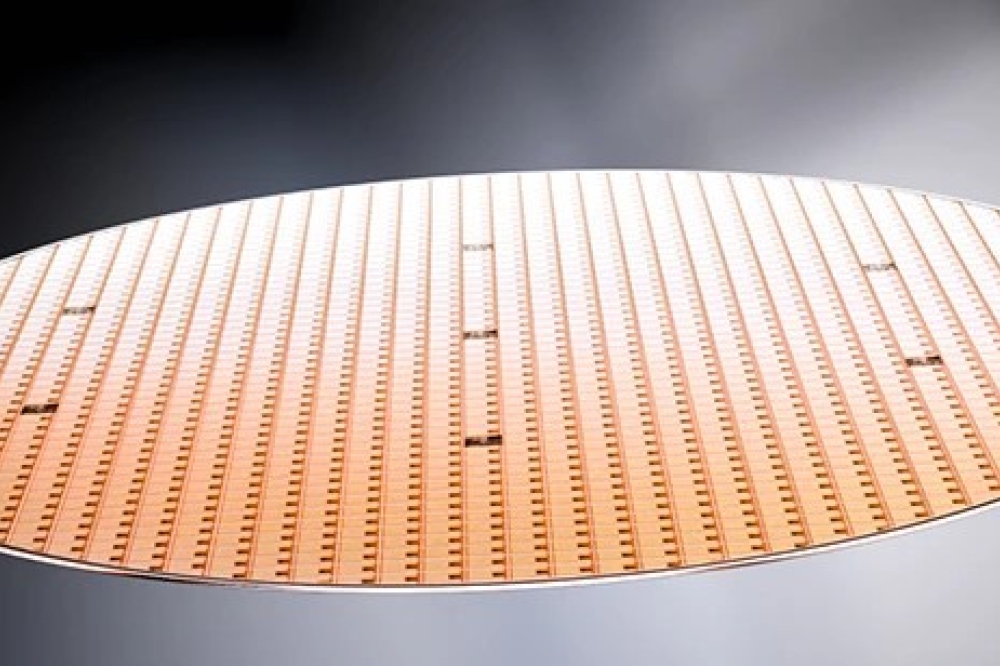
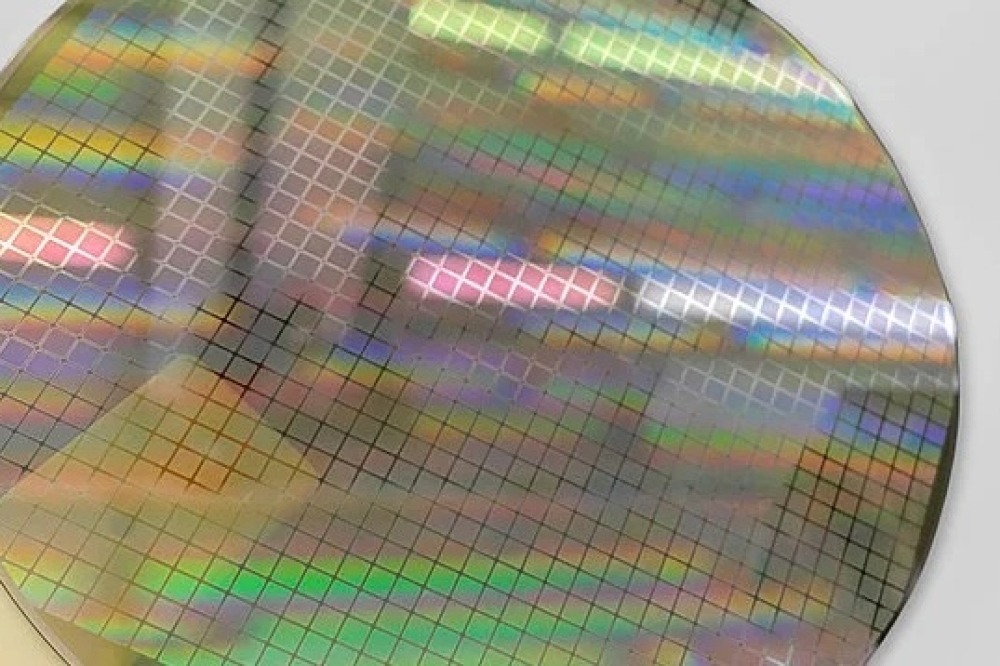
Main image: As-grown 4-inch and 6-inch InP-on-GaAs engineered substrates produced at the Fraunhofer ISE institute.

