Transferrable vertical microLEDs arrays
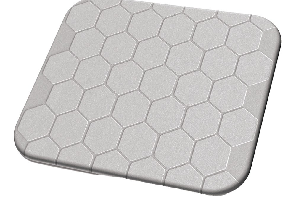
It’s not easy to transfer arrays of incredibly small, vertical GaN-based microLEDs to another platform. But there is a promising solution: selective-area growth of these emitters on hexagonal boron nitride.
BY SURESH SUNDARAM AND ABDALLAH OUGAZZADEN FROM GEORGIA TECH EUROPE
Many are viewing microLEDs as the future of displays. Compared with their organic counterparts, these miniature marvels offer superior efficiencies, higher brightness levels, exceptional contrast, a wide colour gamut, and ease of manufacturability.
Unfortunately, it’s not easy to leverage the standard GaN-based LED growth process and apply it to microLEDs with a top-down fabrication process. That’s because succeeding on this front, which would unlock the door to mass manufacturing, requires addressing a number of key challenges. For example, when etching is employed to define the dimensions of the microLED, this process induces side-wall damage that causes efficiency to plummet with increasing miniaturisation.
Compounding this concern, reliable mass transfer technologies associated with the manufacture of microLED displays are seen as complex and costly. There is a need for devices to be more flexible and offer better heat dissipation, so that they can serve in niche applications.
Figure 1. (a) Structure and scanning electron microscopy
(SEM) images of SiO2 mask deposition by PECVD and hexagonal
patterning on epi-ready sapphire substrates for growth. (b) Structure and SEM image of h-BN grown by
MOCVD on patterned sapphire substrates, showing high-quality BN with wrinkles
on sapphire and granular BN deposits on mask patterns.
The most common foundation for LED production is the sapphire substrate. However, due to its poor thermal and electrical conductivities, as well as its lack of flexibility, there’s a compelling case for trying to remove this particular substrate from the active device package.
Offering an approach doing just this is our team from the Georgia Tech-CNRS Lab at Georgia Tech Europe in Metz, France. We have overcome all the issues just described with a novel growth technology that employs two-dimensional materials and the selective-area growth of GaN. Taking this approach eliminates the need for device isolation and dicing microLED arrays, and thus eliminates the threat of side-wall damage. What’s more, there’s the opportunity for colour tuneability via the size of the microLED, a feature that promises to lead to simple monolithic integration of full-colour displays while avoiding complex issues.
2D materials
Compelling candidates for providing ease of transfer and flexibility for microLED-based displays are those that involve the heterointegration of III-nitrides with two-dimensional (2D) material platforms, such as graphene and hexagonal boron nitride (h-BN). They may be produced by advanced growth methods, such as van der Waals epitaxy and remote epitaxy. While there are many ways to separate sapphire substrates from active devices, standing out for its simplicity is mechanical exfoliation using sacrificial 2D material.
Figure 2. (a) Selective-area growth of a GaN-based LED heterostructure
by MOCVD. Structure and scanning electron microscopy (SEM) image of
microLEDs grown on hexagonal openings. (b) An SEM image after LED’s
sidewall insulation by SiO2 deposition and opening the top surface for a p-type contact.
We are making much progress on this front, having demonstrated the growth of a number of important optoelectronic devices on the h-BN platform – such as LEDs, HEMTs and solar cells – and their transfer to flexible and rigid substrates, foundations that ensure improved optical and electrical performance.
This approach offers several other major advantages, including scalability, with wafer sizes up to 6-inch demonstrated, and the use of thin buffers that trim the thickness of overall device structures to less than 1 µm, cutting the time and energy associated with the growth process. What’s more, our easy transfer to a desired platform ensures a vertical LED architecture that eliminates many front-end processing steps, including mesa-etching. Working with Jeehwan Kim’s group at Massachusetts Institute of Technology, and Young Joon Hong’s team, formerly of Sejong University, we have gone on to demonstrate a vertically stacked microLED display, produced using van der Waals epitaxy. This ground-breaking vertical stack architecture for a full-colour display is incredibly thin – it’s less than 10 mm-thick – and it has a density of 5,500 pixels per inch, sufficient for augmented-reality and virtual-reality headset displays.
Another key breakthrough by our team is the development of a unique bottom-up approach that allows the fabrication of a matrix of transferrable microLEDs, with sizes down to around just 1 µm2. This involves selective-area van der Waals epitaxy, which may solve an inherent issue with the van der Waals epitaxially grown structures: self-delamination during growth/post-growth processing. This concern is addressed while simultaneously providing solutions to the above-mentioned issues associated with microLEDs.
Figure 3. (a) Deposition of a p-type contact, seed layer and
copper electroplating for self-lift-off process and transfer to copper
substrate, and a scanning electron microscopy image of lifted-off arrays
of hexagonal microLEDs on copper and remaining sapphire substrates with
just emptied patterns on it.
The fabrication of our devices starts with patterning sapphire substrates with dielectric layers to the required geometry, in terms of size and shape, before growing GaN-based LEDs on h-BN. We use a standard photolithography process to produce square, hexagonal, and triangular openings in a dielectric, such as SiO2 or SiNx, that’s deposited on a sapphire substrate (an example, hexagonal patterns, is shown in Figure 1(a)). These openings range from around just 1 µm2 to several hundred times this size, and employ dielectric mask widths ranging from 2 µm to 5 µm.
Selective growth?
The use of layered materials, such as h-BN in selective-area growth, is new and unexplored.
To us, the big questions have been whether BN can be grown selectively, and whether the BN platform can be used for GaN selective-area growth. It’s expected that when BN is grown on different substrates, this yields layers of a similar quality, due to the weak van der Waals forces and the absence of polar bonding between the layers and substrates. However, the orientation of the nucleus and the grain sizes of layered material are governed by substrate orientation and crystalline quality.
Our investigations began by growing a thin covering of BN on a sapphire substrate patterned with dielectric materials, such as SiO2 and SiNx. We found that the BN film inside the opening in the patterned area matches the quality of standard h-BN on the sapphire surface, forming semi-hexagonal wrinkles (see Figure 1 (b)). According to localised scanning electron microscopy and transmission electron microscopy images, the BN on the dielectrics has a comparable thickness to that on the patterned area, but has drastically different morphology and crystallinity.
These forms of microscopy reveal that the BN on the dielectric is completely non-crystalline, with a granular morphology (see Figure 1 (b)), while that on sapphire has long-range order. Even though BN grows and conforms over the dielectric pattern, there is an unprecedented difference in lateral quality that exists between the BN that’s grown on sapphire and the BN on the dielectric patterns, and this may lead to the selectivity of the GaN-based device structures.
As previously discussed, the selectivity of GaN that’s grown on h-BN-on-patterned-sapphire substrates is an important and highly attractive feature for designing innovative high-quality microLED device architectures. Merits include the opportunity to avoid Kerf losses, and the elimination of several front-end processing steps, such as mesa etchings to isolate/contact devices.
Figure 4. Variation of current density (at −1 V bias) with the size of
the microLED shows a four-orders-of-magnitude lower current density for
an 8 µm2 size LED. Left inset shows the complete structure of
microLED arrays with an ITO top contact on a copper carrier and right
inset shows the near-field images of the emission from the microLED
arrays of different sizes, with changes from blue to cyan with the size
of the microLED.
The growth of GaN
Pursuing this attractive approach with vigour, we have produced isolated GaN-based microLED structures with sizes down to around just 1 µm2 on h-BN on patterned sapphire substrates. There is complete selectivity, with the growth of GaN only occurring on h-BN on c-sapphire (see Figure 2 (a)).
Although we detected deposits of non-crystalline AlGaN on the BN-on-dielectrics, this ternary does not interfere with the selective-area growth of GaN. Our view is that selective-area van der Waals epitaxy probably promotes the growth of large h-BN and AlGaN grains, leading to more homogeneous lateral coalescence. The upshot is a reduction in the generation of stacking faults in h-BN and dislocations in subsequent GaN/AlGaN layers, compared with growth on a pristine substrate. Thanks to this, there are considerable improvements in electrical and optical performance.
As expected, our approach mitigates the random self-delamination of layers from the substrate during growth or post-growth processing, due to effective strain relaxation within available free lateral surfaces. This lack of self-delamination is promising for realising thick device buffer layers and high-power devices, along with improvement in yield and reproducibility.
We have recorded a noticeable, continuous shift in the emission colour with the size of the microLED. Shrinking dimensions from 32 µm2 to around just 1 µm2 shifts emission from 474 nm to 520 nm. Driving this red-shift is an increase in indium incorporation, as well as a thickness augmentation in quantum wells, associated with changes in surface dynamics that result from selective-area growth. It is possible that by adjusting the geometry of the patterns – that is, the size of the mask and the openings – or by increasing indium content in the quantum well, it may be possible to propel the emission of GaN-based microLEDs to the red. Success on this front could lead to the monolithic integration of red-blue-green vertically stacked active matrix microLED displays.
Figure 5. (a) Optical microscope image of (a) the as-grown sample after
an individual microLED lifted off using a transfer printing machine, and
(b) the microLED transferred onto a flexible substrate.
With our approach, prior to the transfer process, we deposit SiO2 to insulate the sidewalls and define an opening in the top surface, to allow for the addition of a p-type contact (see Figure 2(b)).
Our next step is to transfer our arrays of LEDs to thick copper templates with a self-lift-off and transfer process. This involves the deposition of a titanium (10 nm) and gold (15 nm) seed layer, followed by electroplating a 30 µm-thick layer of copper.
Subsequent heating of this hetero-layer creates thermal stress that induces self-lift-off of the GaN microLED arrays to copper (see Figure 3).
Note that when we transfer microLEDs, with sizes of up to 8 µm2, their structure completely lifts off from the sapphire substrate. Following the transfer, there is no trace of the microLED in patterned sapphire – providing evidence of 100 percent yield – and there are no induced defects or cracks, according to scanning electron microscopy images (see Figure 3). Our microLEDs maintain well defined crystallographic facets and a smooth surface all around, irrespective of the mask width, providing proof of high-quality selective-area growth and effective transfer.
A great strength of smooth side walls, alongside simplistic passivation, is that it solves side wall leakage, one of the major problems with microLEDs. As they get smaller, the maximum external quantum efficiency, which peaks at a higher current density, falls. Such behaviour is common, and has been ascribed to an increase in leakage current and/or Shockley-Read-Hall non-radiative recombination, caused by sidewall defects in smaller chip geometries that are associated with etching damage.
Interestingly, we find that as the size of our microLEDs decreases from 32 µm2 to 8 µm2, the reverse current density under a reverse bias of 1 V continuously falls by around four orders of magnitude (see Figure 4). We attribute this behaviour, which is in stark contrast to that reported for microLEDs fabricated with mesa etching, to the superior crystalline quality of the smooth side walls that comes from selective-area van der Waals epitaxy.
Another attribute of our approach is that it enables the transfer of individual pixels to arbitrary flexible templates using a transfer printing machine (see Figure 5). These transferred microLED arrays or pixels can be addressed by a full front-end process, simplifying the manufacture and integration of microLEDs with any platform, including CMOS and TFT.
Our efforts have created a significant, novel microLED growth technology that mitigates several complex performance and manufacturing issues. The progress that we have made provides a foundation for driving the broader adoption of microLEDs, and bringing down the cost of microLED displays from the premium category.
Our next steps are to make this material structure even better, and to monolithically integrate red, blue and green microLEDs. Offering a reduction in cost at industrial scale, we are hopeful that the 2D materials in microLED manufacturing will reach commercial maturity.
The authors thank Jean Paul Salvestrini, Paul L Voss, Phuong Vuong, Rajat Gujrati, and Ashuthosh Srivastava for their contributions to this work.

