
InGaN full-colour monolithic microLED displays
Toyoda Gosei has unveiled a full-colour InGaN monolithic microLED display produced by stacking and selective removal of light-emitting layers.
This breakthrough builds on this company’s development of a monolithic InGaN LED structure, detailed in a previous paper in Applied Physics Express, published in autumn 2023.
According to the Japanese chipmaker, while displays can be made by combining single-colour monolithic microLEDs emitting in the green, red and blue with a prism – this is a technology that has been commercialised – from cost-reduction and miniaturisation perspectives, a better option is to realise full-colour emission from a single monolithic microLED chip.
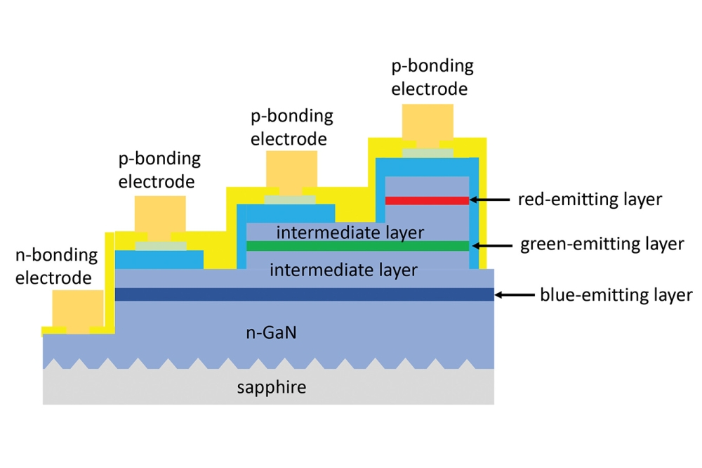
Toyoda Gosei’s previously announced approach to realising this involves stacking layers that emit in the red, green and blue on top of n-type GaN, prior to selective removal of specific portions of these layers, followed by re-growth of a p-type layer (see figure). In the red-emitting region, silicon-doped intermediate layers prevent any electroluminescence from blue-emitting and green-emitting layers that are present. Similarly, in the green-emission region, where red-emitting layers are removed, silicon-doped intermediate layers prevent any electroluminescence from underlying blue-emitting layers.
Building on this full-colour monolithic InGaN technology, engineers at Toyoda Gosei have recently focused on demonstrating displays driven with a passive matrix.
The fabrication of these displays begins depositing an epitaxial structure featuring layers emitting in the blue, red and green. Following selective removal of the light-emitting layers, a p-type layer is regrown to form a multi-colour structure, and devices are then created by forming mesas, adding a p-contact electrode, isolating sub-pixels between rows, and forming a SiO2 passivation layer and n- and p-type bonding layers.
Two additional dry-etching steps ensure that this structure is suitable for a passive matrix display. These two steps involve: removing n-type GaN between the rows (there’s no need to remove n-type GaN between adjacent pixel sub-pixels, due to a passive matrix circuit connecting to a common cathode); and removing the p-type layer between adjacent sub-pixels.
Optical measurements highlight the benefits of partial removal of these layers. When probing a green subpixel, in structures that have not undergone p-type layer removal, holes that are leaking into adjacent subpixels lead to unintended light emission from these regions, resulting in multi-colour emission. Once the p-type layer is removed, leaking is eradicated, and probing the sub-pixel produces emission of only the intended colour.
The team have produced a 3 mm by 3 mm display of 96 by 96 pixels, with pitch of 30 µm by 30 µm. Probing the sub-pixels, which have a light-emitting area of 6 µm by 17 µm, with currents from 10 µA to 200 µA, has verified single-peak emission. External quantum efficiencies for red, green and blue sub-pixels are estimated to be about 0.2 percent, 2 percent and 3 percent, respectively.
The drive voltage for the blue microLED is 0.7 eV higher than that for its red-emitting sibling, due to the difference in bandgap. The green LED has the same drive voltage as the blue variant, a concerning matter thought to be due to processing. Toyoda Gosei’s engineers are investigating this issue.
To operate the chip as a display, the engineers from Toyoda Gosei added two wiring layers by evaporation. These V/Al/Ti layers are separated by a sputtered 400 nm-thick insulating film of SiO2.
Using a microcontroller and drive currents of approximately 200 µA, 100 µA and 100 µA for the red, green and blue subpixels, has enabled the demonstration of a display with a colour gamut of 58 percent of the ITU-R Recommendation BT.2020 and 70 percent of the National Television System Committee standard.
One of the next goals for Toyoda Gosei is to demonstrate displays with sub-pixel sizes smaller than 30 µm. Another aim is to improve the efficiency of red InGaN. Results related to this are due to appear in subsequent publications.
Reference
K. Goshonoo et al. Appl. Phys. Express 18 022003 (2025)


