Exposing SiC defects
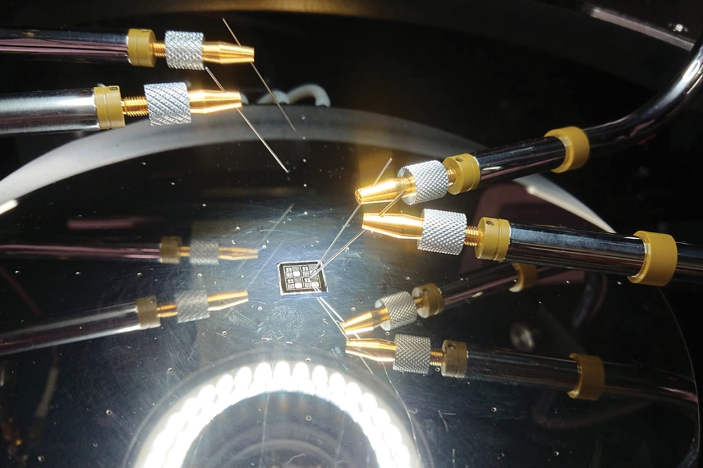
Conductance and optical excitation measurements offer unique insights into interfacial defects in SiC devices.
BY PIYUSH KUMAR, MANUEL BELANCHE AND ULRIKE GROSSNER FROM ETH ZURICH
SILICON CARBIDE is transforming the future of semiconductor devices. Strengths of this wide bandgap matertial include low conduction and switching losses, a high blocking-voltage capability, fast switching, and high operating temperatures. It’s a set of attractive properties that make SiC a compelling candidate for high-power, high-temperature electronics, and radiation-hard applications.
One crucial driver behind the development of SiC power electronics is its similarity to mature silicon transistors, in terms of the manufacturing processes and the device structure – both technologies employ the native oxide SiO2. Thanks to extensive understanding of this dielectric, SiC enjoys a significant advantage over other wide bandgap semiconductors, with its development drawing on existing fabrication processes established for producing silicon devices.
Figure 1. An illustration of a vertical power MOSFET. The inset shows
the region where the current transport occurs from the source to the
drain. Also shown is the location of the border, the interface, and the
bulk traps generated as a consequence of thermal oxidation.
The devil in the defects
Unfortunately, unlocking the promise of SiC demands addressing a number of key challenges. A major one is an imperfect interface between SiC and SiO2 that prevents SiC technology from reaching its full potential. Growth of this dielectric, a thin layer of SiO2, involves thermal oxidation of SiC at high temperatures. During this step many unwanted electrically active defects, commonly referred to as traps, form at the SiO2-SiC interface. These defects drag down channel mobility and capture charges, which cause threshold voltage instabilities, a major concern in the development of SiC MOSFETs.
To address these issues, it is essential to understand the nature of these electrically active defects. Knowing them is the first step to avoiding them.
At the Advanced Power Semiconductor Laboratory, located at ETH Zurich, we are making many important contributions to this objective with conductance and optical excitation measurement techniques. These novel approaches offer new insight into the electrically active defects at the SiO2–SiC interface. Our internally developed optical excitation method uncovers hidden defects near the valence-band edge that tend to be invisible to conventional methods; and our conductance measurements, an improved version of traditional CV and conductance techniques, allow us to study capture dynamics of slow and fast traps in SiC.
This pair of innovative methods is crucial for improving the performance and reliability of SiC devices. By probing SiO2–SiC electrically active defects in a manner that’s not possible with conventional methods, as well as revealing the concentration of these defects, we are able to uncover their energetic and spatial positions and their capture cross sections. These have the potential to improve SiC’s low channel mobility and threshold-voltage instabilities, because these findings expose the source, a key first step to device improvement.
Figure 2. Impact of the linear fitting range on the Dit analysis of the SiC/SiO2 interface. (a) Linear fitting of 1/Cdep2 (red) for four different voltage ranges and their extrapolation to obtain the integration constant K. (b) Impact of the small variations in K on the Dit extraction.
Conventional methods are not enough
Capacitance-voltage (CV) measurements are an established methodology for investigating the interface between the gate oxide and the underlying semiconductor. One of the merits of this approach is its apparent simplicity, in both execution and interpretation. By comparing a low-frequency or quasi-static capacitance curve with a theoretical or high-frequency CV curve, one can extract the density of interface traps. This methodology is known as the C-ψ method.
Although widely used, low capacitance measurements are prone to inaccuracies. They are quite sensitive to systematic errors, coming not only from the influence of the set-up parameters, but also from the evaluation of the density of interface traps. These inaccuracies, which are difficult to detect, have a strong influence on the final results of the density of traps.
Figure 3. The conductance spectrum of the thermally oxidised and NO
annealed sample is shown. The spectrum comprises of three peaks and show
a temperature as well as a bias dependence.
A number of investigations involving extracting the density of interface traps from CV measurements have identified a critical source of errors: the relation between the applied DC bias and the surface potential on the semiconductor. The latter is calculated as a function of the quasi-static capacitance, the oxide capacitance and an integration constant. It is a constant determined from the extrapolation of a linear fit of the surface potential, as a function of the reciprocal of the square of the depletion capacitance (Cdep), which is obtained from the high-frequency CV measurement.
As there are small variations in the integration constant for different fitting ranges, it is tempting to overlook this matter. However, to do so would be a significant oversight, as these small variations in the integration constant compute into a non-negligible shift in the profile of the density of interface traps within the bandgap.
Illustrating this issue is an example of our high-frequency CV measurement, shown in Figure 2 (a). Here, measured values are shown by the red solid curve, and dashed lines correspond to different fitting curves, each using a slightly different range of surface potential. Note that the integration constant, obtained at the intersection of the fitting curve with the x-axis, ranges from 0.1 V to 0.9 V. Variations in the integration constant lead to a significant shift in the curve for the density of interface traps, and could potentially result in a wrong estimation by several orders of magnitude (see Figure 2 (b)). The root cause of this uncertainty is the non-linear behaviour of Cdep-2, observed in the SiC metal-oxide-semiconductor capacitor measurements that differs across samples. We tentatively relate the small curvature to inhomogeneity of the dopant depth profile, but this hypothesis requires further investigation.
Figure 4. The concentration of the three defect groups extracted from
the conductance measurements and their capture cross section as a
function of energy.
The numerous sources of uncertainty inherent in this methodology, and how to avoid them, is a long-winded discussion that highlights the necessity for exploring alternative techniques. This has driven us to develop and implement more robust methods, such as conductance measurements and above-bandgap optical excitation. Read on to discover how these advanced techniques promise to provide a clearer, more accurate understanding of interface and border traps.
Conductance measurements
To account for inaccuracies associated with extracting defect-related information from conventional CV measurements, we have started to investigate interface and border traps with conductance measurements, using a wide frequency range that spans 1 Hz to 10 MHz.
During these measurements, we vary the frequency of the AC signal, the sample’s temperature and the applied DC bias. By tuning these three parameters, we can study the capture dynamics of slow and fast traps in just one measurement. Reducing the minimum measurement frequency to 1 Hz – that’s far, far lower than 1 kHz, often quoted in the academic literature – ensures that we capture very slow traps, which have a capture/emission process that is dominated by tunnelling from the border trap to the conduction band edge of SiC.
Figure 5. The evaluated location of the three defect species extracted using conductance measurements.
Usually, this study is not possible with the conventional high-low CV measurement. There is a price to pay, however, with our novel approach: the extra information extracted from the conductance measurements tends to require longer measurement times.
The samples used for the measurements shown in Figure 3 were produced using thermal oxidation and post-oxidation annealing in a NO environment. This investigation involved recording the conductance as a function of angular frequency for a sample under a fixed DC bias of 0 V at temperatures ranging from 200 K to 233 K (see Figure 3 (a)). The plots uncover three temperature-dependent peaks (see Figure 3 (b)): one at a low frequency, in the range of a few hertz (Peak 01); another at a relatively high frequency, on the order of 10 kHz (Peak 02): and the third at high frequency of around 100 kHz (Peak 03). It worth noting that Peak 01 and Peak 03 show a bias dependence, while the Peak 02 remains almost fixed in frequency for changing DC bias (see Figure 3 (c)).
By varying the temperature during the measurements, we are able to evaluate the parameters associated with these defects. This has enabled us to determine the density of interface traps, the activation energy, and the capture cross-section (see Figure 4). Peaks 01 and 03 result in two clusters with a very small spread in activation energy and capture cross-section, whereas the P02 defects have a spread in both parameters. The first cluster results in defect levels with an activation energy of no more than 0.1 eV with respect to the conduction band edge, and a concentration in the range of 1 x 1012 cm-2 eV-1.
We have determined that this cluster of defects, associated with Peak 01, have a capture cross-section no more than 1 × 10-20 cm2 – that’s several orders of magnitude smaller than that typically expected for bulk defects in SiC. Also featuring in the plots is a second cluster of peak P03, with a very similar activation energy to P01, but a much larger capture cross-section.
Figure 6. Change in capacitance of a MOS-cap under optical excitation with above bandgap light.
According to reports in scientific literature, some defects observed in the conductance measurements would require electrons to tunnel from the conduction band into the oxide, resulting in a reduced effective capture cross-section – it is reduced by a tunnelling probability. This probability ranges from 1 x 10⁻³ to 1 x 10⁻⁶, assuming a potential barrier of 2.7 eV, a tunnelling effective mass that is 0.42 times the mass of the electron, and border traps located between 1 nm and 2.5 nm from the interface. As shown in Figure 4, the P01 and P03 defects have similar values for the activation energy, but the carrier cross-section for P01 is 10-3 to 10-5 times smaller than that for the P03 defect. Assuming that the defects associated with P01 are located around 2.0 nm away from the interface, the resulting carrier cross-section for P01 would be on the same order of magnitude as for the P03 defects.
In short, the P01 and P03 defects exhibit similar intrinsic properties, but due to a spatial separation of around 2.0 nm in the oxide, P01 behaves like a slow trap, while P03 has a relatively fast response, in the range of a few microseconds. The defects associated with P02 show a spread in both the activation energy and the carrier cross-section, attributed to interface defects. We summarise the position of the three defect species in Figure 5.
One of the strengths of conductance measurements is that they provide a deeper understanding of electrically active defects near the conduction band edge. However, in order to obtain a picture that is both more detailed and complete, there’s also a need to closely examine the valence band edge. That’s where above bandgap optical excitation comes into play.
Above bandgap optical excitation
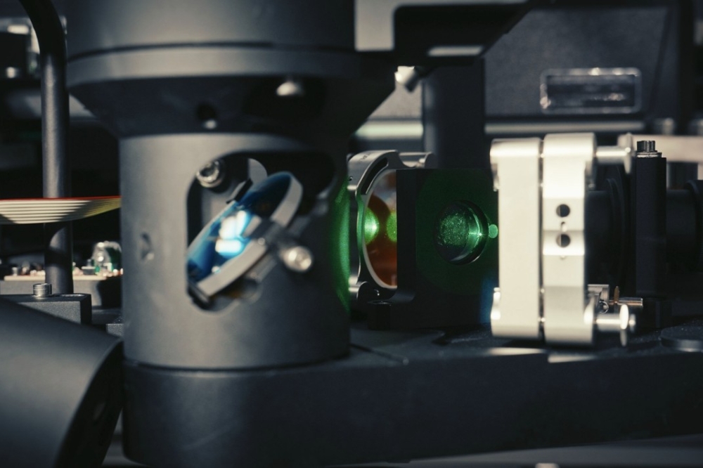
By turning to optical excitation with energy higher than the bandgap, our newly developed technique probes charge capture and emission from the border trap near the valence band edge. While the defects close to the conduction band edge in an n-type sample can be studied with conductance measurements, those close to the valence band edge remain hidden, due to the absence of minority carriers (holes) in SiC metal-oxide-semiconductor capacitors. But we can lift this veil with above-bandgap optical excitation, a technique that generates electron-hole pairs and allows us to study defects close to the valence band edge.
Under optical illumination, using a 365 nm ultraviolet LED that’s emitting above the bandgap of 4H SiC, we observe a rise in the small-signal capacitance of the metal-oxide-semiconductor capacitors. Depending on the sample, the DC bias conditions, and the optical power, rise time ranges from a few seconds to a few hundred seconds. At the start of this experiment, we observe a fast rise in capacitance. But as time progresses, the process slows down – and eventually almost no rise is seen, occurring at a time when effective saturation begins. At this point, we turn off the UV LED. This leads to a sudden drop in capacitance, followed by a slow decay. We view this measurement as complete when the capacitance stops changing for at least 1 minute (see Figure 6).
We attribute the persistent increase in capacitance at the end of optical excitation to the capture of holes at border traps near the valence-band edge. The increase in capacitance is directly proportional to the concentration of captured charges. Due to this phenomena, optical excitation on n-type metal-oxide-semiconductor capacitors allows us to study the concentration of border traps located near the valence-band edge, and ultimately enables us to obtain a more comprehensive understanding of charge capture and emission processes, as well as the intricate dynamics at play within these semiconductor devices.
Our insights must be viewed against a backdrop of advances in SiC device technology, particularly for high-power and high-temperature applications. While there are challenges with electrically active defects at the SiO2–SiC interface, much insight into their nature can be uncovered with our innovative techniques, such as conductance measurements and above bandgap optical excitation.
By understanding the capture dynamics of slow and fast traps near the conduction-band edge and exploring defects near the valence-band edge, we are helping to build a foundation for improving the performance and reliability of SiC devices. Our insights, enhancing our understanding of SiC, will lead to the introduction of more efficient and robust semiconductor technologies.


