GF GaN fab to benefit from $1.5B CHIPS Act funding
Direct funding for GlobalFoundries will create new manufacturing capacity and capabilities
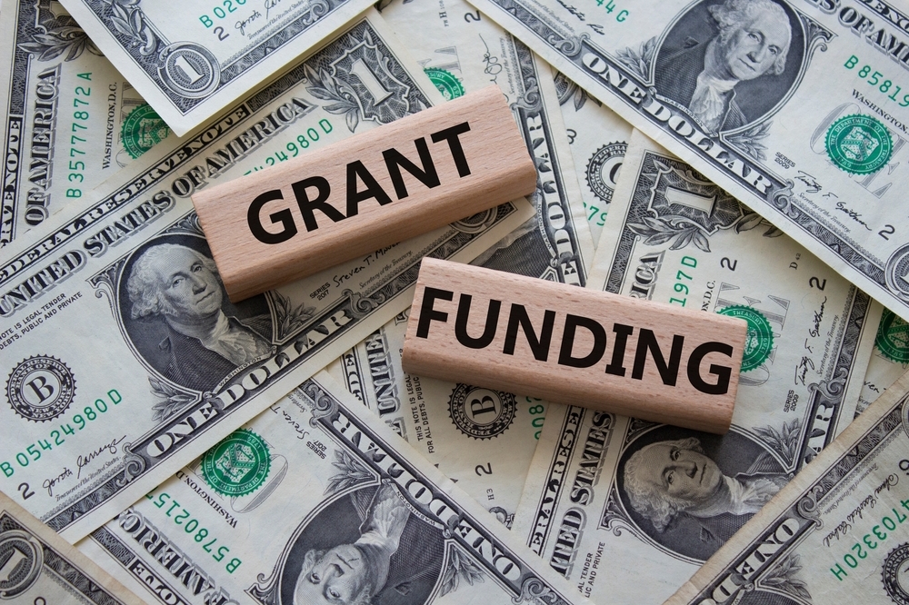
The US Department of Commerce has announced $1.5 billion in planned direct funding for GlobalFoundries as part of the US CHIPS and Science Act. This investment will enable GF to expand and create new manufacturing capacity and capabilities including securing essential GaN chips for automotive, IoT, aerospace, defence, and other vital markets.
GF is the first pure-play foundry to receive a major award (over $1.5 billion) from the CHIPS and Science Act, designed to strengthen American semiconductor manufacturing, supply chains and national security.
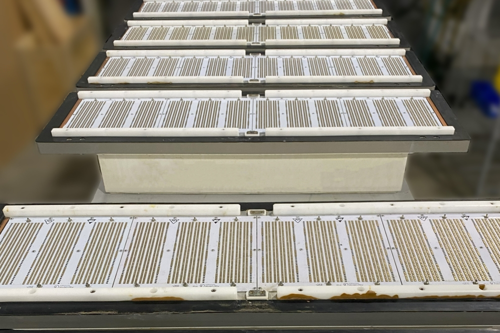
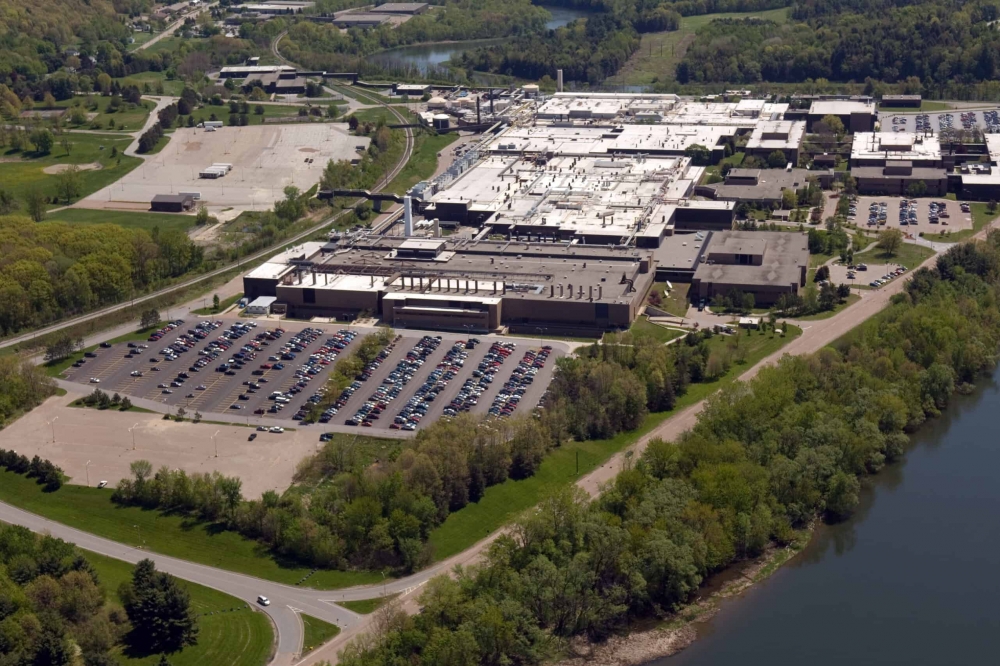
Part of the proposed funding will support the creation of the first US facility capable of high-volume manufacturing of next-generation GaN semiconductors for use in TVs, power grids, data centres, 5G and 6G smartphones and other critical technologies. This will be at the site of GF’s longest continuously operated fab, a 200mm facility in Essex Junction, Vermont. The GaN project was also awarded £35 million in US government funding in October 2023.
The $1.5 billion investment will also help upgrade and expand capacity at GFs existing Vermont facilities. In addition, it will go towards GF’s Malta, NY, fab by adding technologies already in production in GF’s Singapore and Germany facilities geared towards serving the US auto industry.
Overall, based on market requirements and demand, GF plans to invest more than $12 billion over the next 10 plus years across its two US sites through public-private partnerships with support from the federal and state governments as well as from its ecosystem partners, including key strategic customers.
“These proposed investments, along with the investment tax credit (ITC) for semiconductor manufacturing, are central to the next chapter of the GlobalFoundries story and our industry. They will also play an important role in making the U.S. semiconductor ecosystem more globally competitive and resilient and cements the New York Capital Region as a global semiconductor hub,” said Thomas Caulfield, president and CEO of GF. “With new onshore capacity and technology on the horizon, as an industry we now need to turn our attention to increasing the demand for U.S.-made chips, and to growing our talented U.S. semiconductor workforce.”
“Semiconductors are in everything from our cellphones, to refrigerators, to cars, and our most advanced weapons systems, and access to them carries important economic and national security implications. It was the shortages of semiconductors during the COVID-19 pandemic that raised prices for consumers and led to the shutdown of automobile manufacturing sites across the country,” said Secretary of Commerce Gina Raimondo. “Thanks to the CHIPS and Science Act, we're working to onshore these critical technologies in order to bolster the supply of domestic chips that are essential to manufacturing cars, electronics, and national defense systems in New York, Vermont, and states across the country.”
To attract and cultivate a pipeline of semiconductor talent that will be needed in New York and Vermont, GF has announced a new student loan repayment program to help current employees and new recruits pay down student loan debt. The new benefit program is part of the company’s multi-million-dollar investment to strengthen the semiconductor talent workforce by helping to ease the financial burden of higher education and training of the company’s present and future employees.
GF is also partnering with universities and community colleges nationwide to help build a diverse workforce and semiconductor talent pipeline. As part of receiving CHIPS and Science Act funding, GF will continue to invest in and develop new workforce development efforts including curriculum development, internship and apprenticeship programs, K-12 STEM outreach as well as additional education and training programs.