German universities collaborate on GaN-based photonics
Porous GaN research could benefit waveguides, neuromorphic circuits and quantum computing
Researchers at Friedrich Schiller University Jena and Technische Universität Braunschweig in Germany have launched a joint project focusing on porous GaN.
The OptoGaN project—full title 'Highly integrated microphotonic modules in nitride technologies'—has been awarded roughly €600,000 of funding by the Federal Ministry of Education and Research (BMBF) for a three-year term.
The project partners hope to establish three applications with one start-up each as demonstrators. Their research could benefit technologies such as waveguides, neuromorphic computing and the trapped-ion quantum computer operated by the Quantum Valley Lower Saxony network.
The process of manipulating the ions of a quantum computer, for example, still requires large-scale laser systems. If more and more quantum bits are to be incorporated into these computers, their laser systems must become significantly smaller, ideally becoming no larger than a chip. Yet, silicon dioxide—the standard material for waveguides on chips—absorbs the critical wavelengths of light. GaN could provide a solution: the porous material has a low index of refraction and facilitates waveguiding of light to individual ions with minimal losses.
Complementary expertise in handling GaN
The porous semiconductor is the result of a new, selective etching technique that turns electrically conductive areas into air-filled channels referred to as pores. The corresponding electrical contrast is realised through ion implantation with masks.
The researchers think this technique could even open the door to three-dimensional waveguides with complex optical light conduction. GaN and the novel process are compatible with the procedure used to manufacture LEDs and laser diodes to date, thereby making it possible to realise integrated electronic and photonic circuits.
Scientists from Jena and Braunschweig are combining their expertise and specialist equipment for the project. Firstly, researchers in Braunschweig produce the base material, layer by layer. The semiconductor chip is then shipped to Jena for ion implantation. The researchers in Jena dope the chip and make targeted changes to its electronic properties. Finally, the chip returns to Braunschweig, where their chemical etching process creates the final, porous structure.
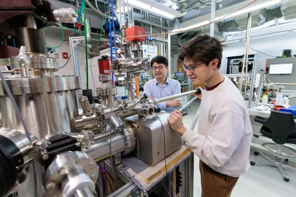
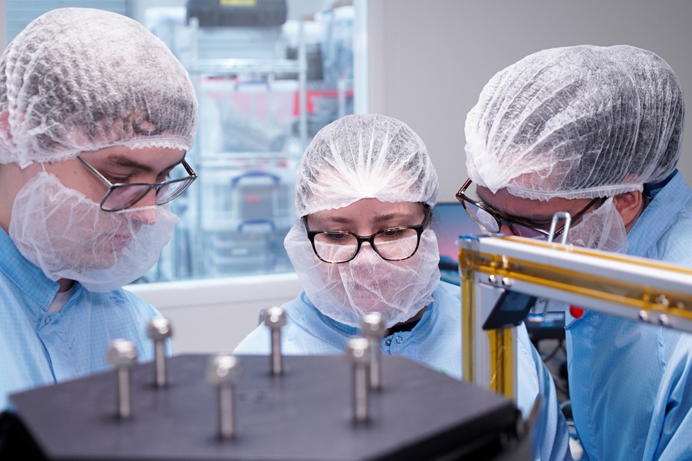
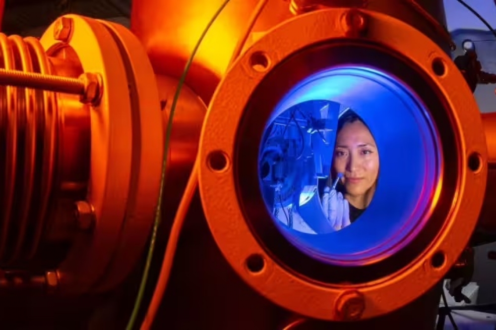
Pictured above: Doctoral candidate Karla Jahaira Paz Corrales experiments with material samples at an ion accelerator