
Thick homoepitaxy on 200 mm SiC
The cost of SiC substrates needs to come down. But are we going to hamper these efforts by imposing limits on the thickness of this foundation?
BY THOMAS KUHR FROM WOLFSPEED
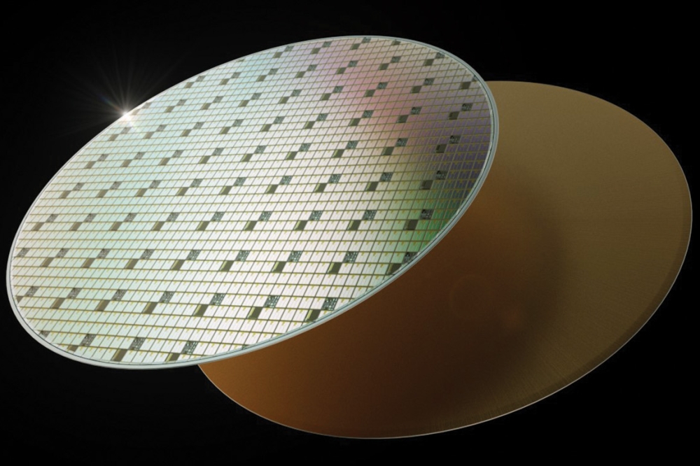
SiC is benefitting from the electric vehicle boon, with uptake of power devices based on this wide bandgap semiconductor enabling higher-efficiency electronics that reduce system losses by 80 percent or more. However, while this is impressive, it is only the tip of the iceberg. As well as its wide band gap, SiC has a high thermal conductivity and an excellent saturation drift velocity, allowing devices made from this material to operate at high electric field densities and serve in many technologies, including high-voltage DC, pulsed power, and solid-state transformers. Using single SiC MOSFET chips that can handle up to 10 kV, or even-higher-voltage bipolar devices, equips designers with the opportunity to simplify systems and reduce resistive-heating losses across many applications.
As SiC continues to demonstrate an improved performance over incumbent technologies, it is facing heavy scrutiny for its higher cost. Within the semiconductor industry, the common solution to this challenge is to move to larger wafers, which divide fixed processing costs over many more devices. This is underway, with SiC substrates currently undergoing a transition from 150 mm to 200 mm diameters. However, in contrast to the silicon industry, which increased wafer thickness with diameter, the SiC industry is considering retaining the 350 mm thickness used for today’s 150 mm-diameter wafers for the 200 mm format.

Figure 1. Comparison of wafer shape maps for 500 µm (left) and 350 µm
(right). Notice that in both cases the full map has not been generated,
though the left scan is more complete. The bow and warp of the 350 mm
wafer is clearly higher and outside the measurement range of the current
tool configuration.
At Wolfspeed, a world leader in SiC substrates and devices, we have been investigating how epitaxial layers of different thicknesses vary in quality, when using wafers with thicknesses of 350 µm and 500 µm. The growth of ‘thin’ SiC layers, used for production of 650 V and 1200 V devices does not tend to result in significant stresses from temperatures profiles, or from differences in doping between the substrate and the epitaxial film. However, when epitaxial layers are thicker and lower doped – they are the two key requirements for higher-breakdown-voltage devices – stresses are magnified, generating new defects and wafer shape concerns.
Additionally, epitaxial defects increase in size and area, because they are often generated at or near the substrate interface and grow commensurately with the film. The compounding effect of greater stress and larger defects, coupled with higher-voltage devices often being larger in size, results in much lower usable area of the wafer, leading to lower die yields and a higher cost per device.

Figure 2. Stitched image map with preliminary inking to estimate usable
area for devices for 115 µm epitaxy on 500 µm-thick 200 mm substrates.
An arbitrary 5 mm x 5mm grid was used for visualisation. Note that not
all defects are correctly identified, but that area effect of gross
defects like triangles can be seen, as shown in the insert.
What could go wrong?
To deepen our understanding of the interaction of thinner substrates and thicker epitaxy, we have investigated the performance of homoepitaxial layers with three different thicknesses, grown on 200 mm SiC substrates that are 350 µm-thick and 500 µm-thick, using two commercially available reactor platforms. Admittedly, the best way to approach this evaluation would be to cut a single boule into multiple substrates with different thicknesses, as this would normalise the starting point for substrate defects – but for this work we used internal production wafers as they became available. We selected doping and thickness targets based on specific device requirements, chosen to hit the lowest resistance at the required breakdown voltage, and we have been able to identify if there are any potential manufacturing limits by utilising a suite of measurements that are part of our standard production fab flow.
One concern during epitaxy is the stability of wafer shape at high growth temperatures. The wafer shape may differ at room temperature and at more than 1600 °C, and thinner wafers may change shape unpredictably. Any variations will adversely affect growth through thickness or doping non-uniformity, and in the worst-case scenario the wafer may break or be ejected from the carrier during processing.
Our results have dispelled this concern when reducing wafer thickness from 500 µm to 350 µm. If anything, the thinner wafers lead to improvements in film thickness and doping uniformity, although this is likely to depend on the reactor furniture design. Note that we need many more growth runs to establish statistically significant conclusions. However, our initial investigations indicate that there are no concerns associated with using thinner 200 mm wafers for the epitaxial growth process.
Due to similarities in the processing chemistry and device design for thin and thick SiC devices, our device fabrication team prefers a similar state for the surface of all epiwafers. To see if this is the case, we scrutinised our material with atomic force microscopy (AFM) and confocal imaging. AFM, useful for gauging short-range roughness, shows a matched performance in roughness, with the average roughness (Ra) less than 0.2 nm for thin and thick films. According to confocal imaging, long-range roughness for thicker films is greater than it is for thin films, with an average roughness (Ra) of around 0.6 nm.

Figure 3. Stitched image maps with preliminary inking to estimate usable area for devices for 74 µm epitaxy on 500 µm and 350 µm thick 200 mm substrates. 5x5 usable areas of 75-85 percent shown.
These finding are independent of substrate thickness, though a bit more roughness is slightly more spatial on the confocal imaging scale. This suggests that like doping and thickness uniformity, surface roughness may be treated as a non-issue with respect to wafer thickness. However, there’s a need to reduce surface roughness in thicker films, and to further refine spatial dependencies.
With thicker epitaxial layers resulting in larger defects and higher film stress, selecting thinner substrates exacerbates the stress problem. Due to this, we were not surprised to find a shape issue when growing thicker epilayers on thinner substrates. Using 200 mm-diameter SiC, growing a 13 µm-thick epilayer on a 500 µm-thick substrate leads to a bow of 20-40 µm; and increasing the thickness to 115 µm, and dropping the doping to the mid-1015 cm-3, increases the bow to around 80 µm. If the substrate is then thinned to 350 µm, bow increases to more than 100 µm, leading to threats of handling errors and wafer breakage during device fabrication processes. While 100 µm of wafer bow may seem miniscule compared with the hundreds of microns of bow that may occur during ion implantation, not all fabrication tools are capable at that starting point. Our view is that more work may be needed to compensate for wafer shape concerns, if substrates that are just 350 µm-thick are going to be used for growing thicker epitaxial layers.
The biggest disadvantages of SiC are its defectivity that’s inherent in its crystal growth process, and the relative ease of defect formation. The defects that are generated during boule growth and reside in the substrate will propagate into the epilayer by either continuation of the growth, or by conversion to other types of defects. The sources of defects could be micropipes, threading dislocations, stacking faults, subsurface damage from surface preparation, or simply a dirty surface from inadequate cleaning; more generally speaking, anything that disrupts the natural stacking of the crystal lattice. For example, a common defect called a ‘triangle’ – it’s a crystal stacking disruption that manifests as a triangular shape visible on the growth surface – increases in size with epitaxial growth, from 0.4 mm-long for 13 µm of epitaxial growth to 3.2 mm for a 115 µm-thick film. You might think what’s the big deal, given that devices are typically 25 mm2 or more in size, so a triangle defect should only affect one or two die.
Well... As we have already mentioned, film stress increases with thickness, and the doping offset between the film and the substrate. Due to this, and the very low formation energy for basal plan dislocations in SiC, it’s possible for defects, such as triangles, to generate basal plane dislocations that glide vertically along the wafer, emanating from the source defect. Consequently, a defect that originally affected just one or two devices may now impact five-to-ten times as many die, slashing yield.
The good news is that by careful management of the temperature distribution on the wafer during epitaxial growth, it’s possible to reduce excessive film stress. Even if this gain comes at the expense of an increase in wafer bow, this enables the processing of thinner wafers without increasing film defectivity.
Unfortunately, not all our measurements went particularly smoothly. Due to incomplete scans, our values for maximum bow on our thin wafers with thick epitaxial layers were initially incorrect. Correcting this error, a simple tooling limitation that can be overcome with minor adjustments, took time and effort.

Figure 4. 10kV die ready for packaging.
We also encountered problems associated with automated inspection of defects, due to inspection algorithms that are trained for a different size defect or a smoother surface. This meant that applying our accurate defect classification and data acquisition to thinner epitaxial layers was initially troublesome for thicker epitaxial films.
Our issues related to wafer bow scans and defect inspection are far from insurmountable, and in the case of defects, they are not even substrate-thickness dependent. However, intervention and development are needed before these techniques can serve in a high-volume manufacturing process.
To summarise, thinner wafers will result in shape concerns that must be addressed, either before or during epitaxial growth. But if the temperature distribution and stresses are effectively managed, additional stress-induced defects should not be problematic. This doesn’t sound too bad… except the predicted yields don’t look great, and the costs are still high.
Illustrating this point, let’s consider 5 mm by 5 mm devices for a 1200 V MOSFET wafer. In this case, the useable area is more than 90 percent. But if thicker epitaxy is needed, the useable area falls to around 70 percent, due to the increased area effect – and if the device size increases, there’s an additional fall in usable area, determined by simple Poisson statistics. Now that SiC wafer with a usable area of more than 90 percent for a 1200 V MOSFETs is potentially below 40 percent for 10 kV MOSFETs – and that’s before the epiwafer has even ever entered a device fab.

Left. High-performance half-bridge 10 kV, 50 mΩ all-SiC power module.
A feasible thickness?
Let’s return to the original question: does thinning the SiC substrate limit the capability of using thicker epitaxial layers to make high-voltage devices? Well maybe… and maybe not. It’s clear that it’s critical to get the wafer shape under control and manage the epitaxial growth stresses, in order to prevent complications during device fabrication and thus keep cost low. To support such efforts, adjustments are needed to ensure continuity of measurement and metrology methods with current best practices and industry standards. But what’s also really importantly is for SiC substrate manufacturers to continue to focus on defect reduction. Without lower defect concentrations, device size and capability or device yield will continue to be trade-offs, and costs will remain high regardless of the optimisation of the epitaxial growth process.
In closing, the drive for thinner SiC substrates will continue, because reducing their cost remains a huge motivator. Against this backdrop, innovators will find ways to deal with wafer shape, and substrate manufacturers will continue to decrease defect density, helping to improve device yields and trim costs.
Out of shear technological need, adoption of higher-voltage devices will continue to rise, with 10 kV MOSFETs eventually paving the way for even higher voltage IGBTs. The SiC revolution will continue!


